Category: Projects and Founding

New article in Physical Review Materials

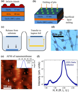
Direct observation of large-area strain propagation on free-standing nanomembranes Investigations on epitaxial nanostructures with size of tens of nanometers have been a challenging issue for techniques that present high strain sensitivity but restricted spatial resolution. This is the case of recently developed x-ray nanoprobe techniques. Despite its inherent nondestructive character, submicron x-ray spots have only …

Continue reading

New publication in “Journal of Physical Chemistry C”

Strain Tuning in Graded SiGe on Insulator: Interplay between Local Concentration and Nonmonotonic Lattice Evolution after Ge Condensation Germanium condensation has proven to be a reliable route for obtaining smoothly graded composition SiGe layers with good reproducibility and reduced defect density. The process is known as a crucial tool to induce well-defined strain on Si …

Continue reading

New article in “Nanotechnology” is out: Imaging the electrostatic landscape of unstrained self-assemble GaAs quantum dots

Unstrained GaAs quantum dots are promising candidates for quantum information devices due to their optical properties, but their electronic properties have remained relatively unexplored until now. In this work, we systematically investigate the electronic structure and natural charging of GaAs quantum dots at room temperature using Kelvin probe force microscopy (KPFM). We observe a clear …

Continue reading

Featured by SPBMat

Our last article has been featured by the Brazilian Material Research Society: See their post “Engenharia de estrutura de banda usando a geometria de tubos enrolados.” Thanks for this.  

New article in ACS Applied Nano Materials

After seeing the effect the first time 10 years ago in old samples, we finally figured out what was happening. See out latest results in ACS Appl. Nano Mater. with the title “Rolled-Up Quantum Wells Composed of Nanolayered InGaAs/GaAs Heterostructures as Optical Materials for Quantum Information Technology”:  Strain-based band structure engineering is a powerful tool …

Continue reading

New article: Band structure engineering in strain-free GaAs mesoscopic structures

We investigate the optical properties of strain-free mesoscopic GaAs/Al(x)Ga(1-x)As structures (MGS) coupled to thin GaAs/A(x)Ga(1-x)As quantum wells (QWs) with varying Al content (x). We demonstrate that quenching the QW emission by controlling the band crossover between AlGaAs X-point and GaAs Gamma-point gives rise to long carrier lifetimes and enhanced optical emission from the MGS. For …

Continue reading

New article: Scanning Tunneling Measurements in Membrane-Based Nanostructures

Our new article: “Scanning Tunneling Measurements in Membrane-Based Nanostructures: Spatially- Resolved Quantum State Analysis in Postprocessed Epitaxial Systems for Optoelectronic Applications” is out in ACS Appl. Nano Mater. Nanoscale heterostructure engineering is the main target for the development of optoelectronic devices. In this sense, a precise knowledge of local electronic response after materials processing is …

Continue reading

Article accepted in Nanoscale

In-place bonded semiconductor membranes as compliant substrates for IIIV compound devices Overcoming the critical thickness limit in pseudomorphic growth of lattice mismatched heterostructures is a fundamental challenge in heteroepitaxy. On-demand transfer of light-emitting structures to arbitrary host substrates is an important technological path for optoelectronics and photonics devices implementation.  The use of freestanding membranes as …

Continue reading

Why the State of São Paulo is good in science and why it is important

The is a very nice article in Nature  discussing, why the state of SP is so good in science. Indeed, the state alone is responsible for more than 50% of Brazilian science production and  the leading place in South America. That this is of great importance for the country and the society is shown on …

Continue reading

Back making rolled-up tubes

We are back to make rolled-up InGaAs/GaAs nano- and microtubes. We stopped doing the process for more than a year, but now is the time to strongly restart the activity. The light microscopy image shows one of our first process. The MBE grown sample coming from our machine rolls nicely, but we have to optimize …

Continue reading