
 Our publication investigating the structure of overgrown transferred silicon membranes is finally out: Have a look to “Silicon Nanomembranes with Hybrid Crystal Orientations and Strain States“.
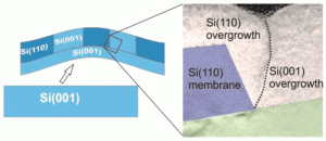
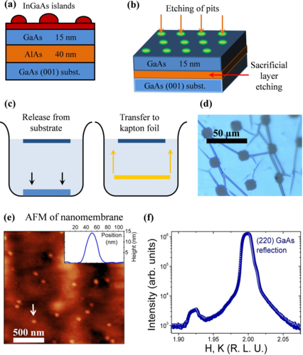
Methods to integrate different crystal orientations, strain states, and compositions of semiconductors in planar and preferably flexible configurations may enable nontraditional sensing-, stimulating-, or communication-device applications. We combine crystalline-silicon nanomembranes, patterning, membrane transfer, and epitaxial growth to demonstrate planar arrays of different orientations and strain states of Si in a single membrane, which is then readily transferable to other substrates, including flexible supports. As examples, regions of Si(001) and Si(110) or strained Si(110) are combined to form a multicomponent, single substrate with high-quality narrow interfaces. We perform extensive structural characterization of all interfaces and measure charge-carrier mobilities in different regions of a 2D quilt. The method is readily extendable to include varying compositions or different classes of materials.
Authors: Shelley A. Scott, Christoph Deneke, Deborah M. Paskiewicz, Hyuk Ju Ryu,
Angelo Malachias, Stefan Baunack, Oliver G. Schmidt, Donald E. Savage, Mark A. Eriksson,
and Max G. Lagally
ACS Appl. Mater. Interfaces, 2017, 9 (48), pp 42372–42382
DOI: 10.1021/acsami.7b14291

DOI: 10.1002/smll.202105424")

DOI: 10.1088/1361-6528/ac47ce")


DOI: 10.1088/1361-6528/ace4d1")
, 3140–3147 (2021)
DOI: 10.1021/acsanm.1c00354")

DOI: 10.1088/1361-6528/ab7d74")


