
In-place bonded semiconductor membranes as compliant substrates for IIIV compound devices
Overcoming the critical thickness limit in pseudomorphic growth of lattice mismatched heterostructures is a 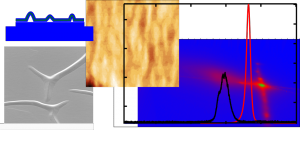 fundamental challenge in heteroepitaxy. On-demand transfer of light-emitting structures to arbitrary host substrates is an important technological path for optoelectronics and photonics devices implementation. The use of freestanding membranes as compliant substrates is a promising approach to address both issues.
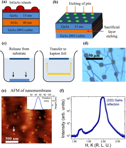
In this work, the feasibility of using released GaAs/InGaAs/GaAs membranes as virtual substrates to thin films of InGaAs alloy is investigated as a function of the Indium content in the films. Growth of flat epitaxial films is demonstrated with critical thickness beyond typical values regarding growth on bulk substrates. Optically active structures are also grown on these membranes with strong photoluminescence signal and clear red shift for an InAlGaAs/InGaAs/InAlGaAs quantum well. The red shift is ascribed to strain reduction in the quantum well due to the use of completely relaxed membrane as substrate. Our results demonstrate that such membranes constitute a virtual substrate allowing further heterostructure strain engineering not possible by other post-growth methods.
Authors: Ailton Jose Garcia Junior, Leonarde N. Rodrigues, Saimon Filipe Covre da Silva, Sergio L. Morelhao, Odilon D. D. Couto Jr., Fernando Iikawa and Christoph Deneke
Journal: Nanoscale 11, 3748-3756 (2019)
As featured on the page of the IFGW

DOI: 10.1002/smll.202105424")

DOI: 10.1088/1361-6528/ac47ce")


DOI: 10.1088/1361-6528/ace4d1")
, 3140–3147 (2021)
DOI: 10.1021/acsanm.1c00354")

DOI: 10.1088/1361-6528/ab7d74")


