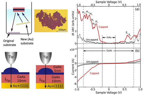
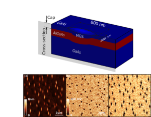
 Unstrained GaAs quantum dots are promising candidates for quantum information devices due to their optical properties, but their electronic properties have remained relatively unexplored until now. In this work, we systematically investigate the electronic structure and natural charging of GaAs quantum dots at room temperature using Kelvin probe force microscopy (KPFM). We observe a clear electrical signal from these structures demonstrating a lower surface potential in the middle of the dot. We ascribe this to charge accumulation and confinement inside these structures. Our systematical investigation reveals that the change in surface potential is larger for a nominal dot filling of 2 nm and then starts to decrease for thicker GaAs layers. Using k · p calculation, we show that the confinement comes from the band bending due to the surface Fermi level pinning. We find a correlation between the calculated charge density and the KPFM signal indicating that k · p calculations could be used to estimate the KPFM signal for a given structure. Our results suggest that these self-assembled structures could be used to study physical phenomena connected to charged quantum dots like Coulomb blockade or Kondo effect.
Evandro Martin Lanzoni, Saimon F Covre da Silva, Matthijn Floris Knopper, Ailton J Garcia, Carlos Alberto Rodrigues Costa and Christoph Deneke
Nanotechnology 33, 165701 (2022)

