The Materials Preparation and Characterization Laboratory specializes in creating and analyzing semiconductor materials and nanostructures—the tiny building blocks that power modern electronics and photonics. Our core work involves III-V semiconductors (materials made from elements in columns III and V of the periodic table, like gallium arsenide), which are essential for high-speed electronics and advanced light-based technologies.
We harness these special materials to create:
- Nanomembranes for 2D and 3D Self-Forming Objects: Nanomembranes are ultra-thin, flexible sheets of semiconductor material that can be used as compliant substrates. They can spontaneously roll or fold into complex three-dimensional shapes used to create microscopic optical devices by strain-engineering the initial heterostructure.
- Optical Emitters and Photonic Structures: Devices that efficiently produce or control light, which are crucial for lasers, LEDs, and future optical circuits. Thereby, we are currently interested in the fabrication of single-photon emitters and sources essential for quantum communication.
We also focus on integrating different materials into these nanostructures to unlock new and enhanced functionalities.
Research topics
We have deep, long-standing experience in cutting-edge fabrication techniques:
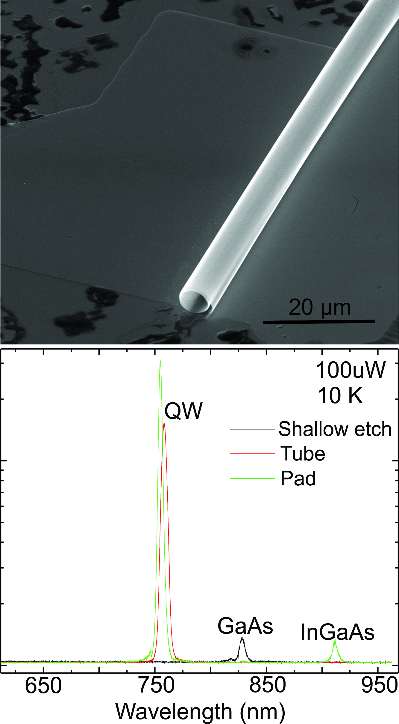
- . Rolled-Up Nanotubes and Micro-Optics
We are experts in rolling up our ultra-thin materials into nanotubes or micro-tubes. These tiny cylinders can act as highly efficient photonic structures—miniature light traps or resonators—that have potential applications in advanced sensors and communication.
- Molecular Beam Epitaxy (MBE)
We use a sophisticated technique called Molecular Beam Epitaxy (MBE) to grow perfect, atomic-layer-by-atomic-layer III-V heterostructures (layered materials). This technique gives us ultimate control over the material’s properties.
- Virtual Substrates: We have pioneered a method where we use released III-V nanomembranes as virtual substrates to build even more complex and higher-quality layered structures on top.
- Self-Assembled Structures: Our work also includes growing naturally forming structures like self-assembled quantum dots (tiny semiconductor islands that act like artificial atoms) and using techniques like local droplet etching to create nanoscale patterns.

Characterization
To ensure our materials are perfect, we use a suite of powerful characterization tools:
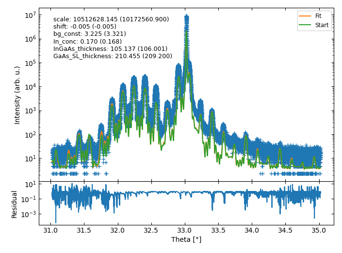
- X-ray Diffraction (XRD): This technique uses X-rays to precisely measure the spacing and quality of the atomic layers in our structures.
- Atomic Force Microscopy (AFM): Like a record player, the AFM uses a tiny needle to map the surface topography of our materials at the nanoscale.
- Scanning Electron Microscopy (SEM): The SEM uses a beam of electrons to create highly detailed, high-magnification images of the material’s surface structure.
- Photoluminescence (PL) Measurements: This essential technique helps us understand how efficiently our materials emit light, which is critical for their application in optical devices.
Complimanetary techniques
To understand and interpret our experimental results, we carry out a wide variety of computer-based simulation techniques using commercial or self-developed software. We are active in:
- Monte Carlo simulation: Random walk of atoms in surface energy potential to understand epitaxial growth.
- Finite-difference time-domain simulations: Understanding how electric fields and light propagate inside our micro- and nanostructures.
- k dot p calculations: Solving the wavefunctions of electrons inside a potential. We use this to understand the light emission of our nanostructures like quantum dots and quantum wells.
Group History
Research in crystallography in IFGW was initiated by Professor Stephenson Caticha-Ellis (1930-2003), born in the small city of Melo, Uruguay. Caticha studied at Glasgow University and the Cavendish Laboratory at Cambridge University (UK) and did internships at the University of Paris (France), the Georgia Institute of Technology, and the Polytechnic Institute of Brooklyn (USA). He arrived in Brazil in the late 1960s, where he worked first at the Institute of Atomic Energy of St. Paul (now, IPEN, Institute of Energy and Nuclear Research), especially with neutron diffraction. In the early 1970s, he moved to the Institute of Physics Gleb Wataghin Unicamp, this time using X-ray diffraction.
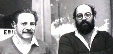
Professores Stephenson Caticha Ellis e Lisandro Pavie Cardoso em foto de 1984 na porta do LPCM.
A group formed and then returned to the study of the crystal defects, particularly using the multiple diffraction X-rays, which was an expert using the bases of the kinematics and dynamics of diffraction X-rays. Thus was created the group of Crystallography of the Institute of Physics Gleb Wataghin, which had the important contribution of several other researchers who passed through it.
After Caticha retired in 1991, with the split of the group, one of the teams – the X-ray Diffraction Laboratory (LDRX today LPCM) – continued to explore the potential of multiple diffraction of X-rays and associated techniques, particularly for single crystals, thin films and semiconductor epitaxial structures.
From 2017 on, the group includes a new generation of professors. With them, the scope and topics of research widen, but they also engage with the traditional research carried out using x-ray diffraction to solve problems of materials science, physics, or related fields.
Finally, in 2022 the last research focused on pure diffraction left the group, and we have changed our focus towards the growth and fabrication of semiconductor nanostructures and devices based thereon.


