New article in “Nano Letters”

Low-Density InGaAs/AlGaAs Quantum Dots in Droplet-Etched Nanoholes

Over the past two decades, epitaxial semiconductor quantum dots (QDs) have demonstrated very promising properties as sources of single and entangled photons on-demand. Among different growth methods, droplet etching epitaxy has allowed the growth of almost strain-free QDs, with low and controllable surface densities, small excitonic fine structure splitting (FSS), and fast radiative decays. Here, we extend the technique to In(Ga)As QDs in AlGaAs, thereby increasing the achievable emission wavelength range beyond that accessible to GaAs/AlGaAs QDs while preserving some of the key advantages of this growth method. We observe QD densities of ∼0.25 μm–2, FSS values as small as 3 μeV, and short radiative lifetimes of ∼300 ps, while extending the achievable emission wavelength to ∼900 nm at cryogenic temperatures. We envision these QDs to be particularly suitable for integrated quantum photonics applications.

Saimon F. Covre Da Silva, Ailton J. Garcia Jr., Maximilian Aigner, Christian Weidinger, Tobias M. Krieger, Gabriel Undeutsch, Christoph Deneke, Ishrat Bashir, Santanu Manna, Melina Peter, Ievgen Brytavskyi, Johannes Aberl, Armando Rastelli

Nano Lett. 2026
DOI: 10.1021/acs.nanolett.5c04426

New article in Nanoscale

A new article from our collaboration with the UFV is out in Nanoscale:

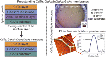
Lattice stability and elastic evolution of CdTe membranes fabrication using a III-V heterostructures as a substrate

CdTe is a key binary compound for II-VI semiconductor systems since the precise control of its growth over different semiconductor materials of different orientations provides a general roadmap for telluride compounds, ranging from optically active layers to diluted magnetic semiconductors and topological insulators. The precise understanding of its epitaxy, film orientation and built-in strain is crucial for II-VI layer integration with commercial hosting substrates used for the latest semiconductor process nodes such as Si and GaAs. In this work, we show that it is feasible to use CdTe:GaAs/InGaAs/GaAs released membranes, yielding high-quality crystalline layers. A combination of Raman scattering and X-ray diffraction results provide a concise scenario of evolution along different growth stages. Surface roughness and contact potential are evaluated by atomic force and Kelvin-probe microscopy, respectively. The coexistence of faceting types (001) and (111) becomes clear using AFM and KPFM near the edge of a CdTe membrane. At such edges the local cleavage of the membrane is probed, exposing several layer steps and reflecting the growth history of CdTe. In this condition, KPFM clearly differentiates faceting (throughout contact potential difference) more accurately than height profiles, allowing a qualitative explanation of the nucleation evolution in our system. Finally, the occurrence of a 4% in-plane interfacial compressive strain is observed by nanomembrane release and modelling with finite element methods. The results showing the flexibility of high-quality CdTe layers here can improve optoelectronic integration of II-VI semiconductors.

Wesley Fiorio Inoch, Eduarda Policarpo, Misael Cesar Isaac Muniz, Angelo Malachias, Gilberto Rodrigues-Junior, Sukarno Olavo Ferreira, Christoph Deneke, Bráulio Soares Archanjo, Erika Peixoto Pimenta Peixoto Pimenta, Luciano Moura, Eduardo Nery Duarte Araujo and Leonarde do Nascimento N. Rodrigues

Nanoscale, 2025, 17, 15279 – 15288
DOI: https://doi.org/10.1039/D4NR05029K

New Grant in Quantum Technology

Our group member Saimon Filipe Covre da Silva won a Young Investigators (JP) grant “Solid state single-photon sources for telecom frequencies” from FAPESP (24/08527-2) for quantum technologies in the Program in Quantum Technologies (QuTIa). The project will be realized here in the IFGW, and we have the pleasure of hosting him for the time of the project.

Abstract

Local droplet etching (LDE) has been established as a powerful method to produce solid state semiconductor single photon and entangled photons pairs inherently compatible with established semiconductor technology. In this proposal, we aim to develop a single photon source emitting at telecom C-band, extending the LDE fabrication approach from the (In)GaAs/AlGaAs system to the III-Sb material system. This would enable the integration of quantum communication already demonstrated for the visible range to be used in the existing optical fiber network, paving the way for the easy use of quantum technologies on a daily basis.

New article in Phys. Rev. Materials

Direct observation of large-area strain propagation on free-standing nanomembranes

Investigations on epitaxial nanostructures with size of tens of nanometers have been a challenging issue for techniques that present high strain sensitivity but restricted spatial resolution. This is the case of recently developed x-ray nanoprobe techniques. Despite its inherent nondestructive character, submicron x-ray spots have only been successfully applied to the study of individual nanostructures which are either strain free or present extremely mild spatial lattice parameter gradients. Such limitation, with an uttermost barrier given by the diffraction limit, leads to voxel or pixel sizes between 5 and 10 nm obtained in coherent diffraction imaging or ptychographic reconstructions of real-space objects. Whenever the strain field of a nanostructure is successfully reconstructed from reciprocal space measurements, it cannot vary considerably in short distances since this would induce diffraction peak broadening and cause abrupt phase variations, leading to convergence issues on reconstruction algorithms. Here we show how epitaxial systems with large lattice mismatch and appreciable interfacial strain can be identified and directly analyzed throughout their strain field propagation in nanometer-thin crystalline membrane platforms, using the InGaAs/GaAs Stranski-Krastanov system as a model. The strain-induced footprint becomes observable along a few microns if the membrane thickness is comparable to the nanostructure size. It is possible to retrieve both interfacial strain and nanostructure size by probing individual objects.

Yuri Bernardes, Lucas A. B. Marçal, Barbara L. T. Rosa, Ailton Garcia, Jr., Christoph Deneke, Tobias U. Schülli, Marie-Ingrid Richard, and Angelo Malachias

Phys. Rev. Materials 7, 026002

DOI: 10.1103/PhysRevMaterials.7.026002

New publication in “Journal of Physical Chemistry C” by group member

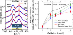
Strain Tuning in Graded SiGe on Insulator: Interplay between Local Concentration and Nonmonotonic Lattice Evolution after Ge Condensation

Germanium condensation has proven to be a reliable route for obtaining smoothly graded composition SiGe layers with good reproducibility and reduced defect density. The process is known as a crucial tool to induce well-defined strain on Si or SiGe layers with potential use in semiconductor devices. In this work, we show that starting from a low concentration Si0.92Ge0.08 layer grown on top of a crystalline Si(001) on SOI substrates, we can reach desirable concentration with a nonmonotonic interplay on in-plane and out-of-plane strain. The Ge concentration is evaluated by a combination of ultralow energy secondary ion mass spectroscopy (ULE-SIMS) and synchrotron X-ray measurements (diffraction and reflectivity). After the evaluation of Ge content, the strain-sensitive process of rolling up tubes from the flat layers is used and combined with X-ray diffraction to provide a concise scenario of the strain evolution along an in-growth oxidation series, pointing out the conditions that maximize strain, as well as its fading, as the Ge content rises.

Gilberto Rodrigues-Junior, Francesca Cavallo, Christoph Deneke, and Angelo Malachias

J. Phys. Chem. C 2022, xxxxx

DOI: 10.1021/acs.jpcc.2c05702

Master student for CNPq position

With the granting of the CNPq project (408219/2022-0) from call “Chamada CNPq/SEMPI/MCTI Nº 57/2022 – MESTRADO OU DOUTORADO EM COMPUTAÇÃO QUÂNTICA, FOTÔNICA INTEGRADA E INTELIGÊNCIA ARTIFICIAL”, Prof. Christoph Deneke has an open position for a master student to work in the area of photonics.

The position is available from now on to start in the next entrance to PostGraduation of the IFGW/Unicamp.

Fell free to contact Ch. Deneke.

Renovation of lab space

With the money from the FAEPEX project 2102/21, we could carry out some long needed renovation of the lab space. In January 2022, we renewed the chemical working places, created a common working space as well as improved the overall installations of the lab.

We will also clean out some old instruments to do a fresh restart of the area for everyone, now that we are back to the university.

New article by group member

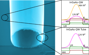
Strain-based band structure engineering is a powerful tool to tune the optical and electronic properties of semiconductor nanostructures. We show that we can tune the band structure of InGaAs semiconductor quantum wells and modify the helicity of the emitted light by integrating them into rolled-up heterostructures and changing their geometrical configuration. Experimental results from photoluminescence and photoluminescence excitation spectroscopy demonstrate a strong energy shift of the valence-band states in comparison to flat structures, as a consequence of an inversion of the heavy-hole with the light-hole states in a rolled-up InGaAs quantum well. The inversion and mixing of the band states lead to a strong change in the optical selection rules for the rolled-up quantum wells, which show vanishing spin polarization in the conduction band even under near-resonant excitation conditions. Band structure calculations are carried out to understand the changes in the electronic transitions and to predict the emission and absorption spectra for a given geometrical configuration. Comparison between experiment and theory shows an excellent agreement. These observed profound changes in the fundamental properties can be applied as a strategic route to develop novel optical devices for quantum information technology.

Leonarde N. Rodrigues, Diego Scolfaro, Lucas da Conceição, Angelo Malachias, Odilon D. D. Couto, Jr, Fernando Iikawa, and Christoph Deneke

ACS Appl. Nano Mater., online (2021)
DOI: 10.1021/acsanm.1c00354

Research was supported by FAPESP and CNPq.

The article was featured by the SPBMat – here the Portuguese post.

Presentation of PIBIC project – Pedro Carneiro

For the annual PIBIC congress, Pedro made a video poster of his work: “Desenvolvimento de um experimento de quantificação da concentração de elementos por fluorescência de raios X e aplicação para o estudo de modelos de epilepsia em roedores”.

Presentation of PIBIC project – Gabriel Gomes

For the annual PIBIC congress, Gabriel made a video poster of his work “Fabricação e caracterização de membranas baseadas em nanoestruturas semicondutoras”.