
Our new article: “Scanning Tunneling Measurements in Membrane-Based Nanostructures: Spatially- Resolved Quantum State Analysis in Postprocessed Epitaxial Systems for Optoelectronic Applications” is out in ACS Appl. Nano Mater.
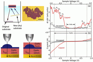 Nanoscale heterostructure engineering is the main target for the development of optoelectronic devices. In this sense, a precise knowledge of local electronic response after materials processing is required to envisage technological applications. A number of local probe techniques that address single nanostructure signals were satisfactorily employed in semiconductor epitaxial systems. In this work we show that the use of chemically etched semiconductor nanomembranes allows carrying out scanning tunneling spectroscopy (STS) measurements in a postprocessed system which was otherwise studied mainly under in situ conditions that differ from the operational regime. We were able to acquire STS spectra with energy level resolved response on InAs quantum dots grown within a 15 nm-thick GaAs single-crystalline film transferred to an Au(111) surface. The presence of a native oxide layer does not affect the result, keeping the reliability of the usual ultra high vacuum (UHV) procedures. The use of nanomembranes also opens up the possibility of tailoring properties via additional variables such as nanomembrane thickness and surface charge depletion. Our method is applicable to a broad class of postprocessed layers extracted in nanomembrane format from epitaxial systems that are potential candidates for optoelectronic applications.
Authors: Barbara L. T. Rosa, Carlos A. Parra-Murillo, Thais Chagas, Ailton J. Garcia Junior, Paulo S. S. Guimarães, Paulo S. S. Guimarães, Ch. Deneke, Rogerio Magalhães-Paniago and Angelo Malachias
ACS Appl. Nano Mater. 2, 4655-4664,(2019)
DOI: 10.1021/acsanm.9b01124

DOI: 10.1002/smll.202105424")

DOI: 10.1088/1361-6528/ac47ce")


DOI: 10.1088/1361-6528/ace4d1")
, 3140–3147 (2021)
DOI: 10.1021/acsanm.1c00354")

DOI: 10.1088/1361-6528/ab7d74")


