
 My research is centered around advanced 2D materials – these include semiconductor freestanding membranes as well as materials like graphene and TMDs. I am interested in synthesis, fabrication, and application of these materials and structures with a long-standing history of using molecular beam epitaxy for the growth of III-V heterostructures and self-assembly like quantum dots. To produce rolled-up tubes and other freestanding semiconductor structures, I use optical lithography. For characterization techniques, I have experience in various microscopy techniques (AFM, KPFM, SEM and TEM), x-ray diffraction (XRD) and optical characterization (PL, Raman and PLE).
Recently, I have a stronger emphasis on simulation and model techniques to explain results. I carry out band structure calculations (k.p using nextnano++) to understand the optical transitions in curved heterostructures. Furthermore, I have experience in finite difference time domain (FTDT using MEEP) calculations simulating optical resonators based on rolled-up tubes. Besides this, I use Python with various packages to model XRD data from flat layers, powders or rolled-up tubes as well as to carry out Monte Carlo simulations of growth processes.
Deterministic release and rearrangement of nanomembranes
In the last years, freestanding membranes have been established as a building block for nanotechnology. Investigated structures include stretchable electronics, solar cells, wrinkled semiconductor membranes for various applications as well as rolled-up and folded three-dimensional micro- and nano-objects.
Rolled-up tubes as building blocks for nanotechnology
We are working on emerging device structures based on rolled-up membranes (supported by FAPESP and CNPq projects). In the last decade, these structures were used as optical resonators, sensors or suggested as x-ray wave guides. The structures are fabricated by growing a strained heterostructure by molecular beam epitaxy, defining a pattern using optical lithography followed by selective underetching releasing the layer system. The tube forms by self-assembly due to strain relaxation of the initial layer system. We want to understand, how the special strain state of the tube wall influences the physical properties of integrated light emitters, e.g. quantum wells. Using the possibility to form hybrid radial superlattices of unique material combinations, we intend to integrate new magnetic or plasmonic functionality.
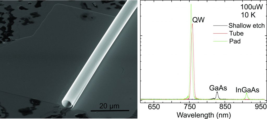
The scanning electron microscopy image above shows a rolled-up micro-tube with a quantum well integrated into the tube walls. The photoluminescence spectrum on the left demonstrates (obtained in collaboration with the GPO of the IFGW), how the emission of the quantum well shifts due to the roll-up process and strain relaxation.
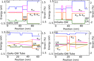
The shift can be understood using band structure calculations as demonstrated above. Using the XRD determinate strain profile of the flat layers and rolled-up tube, we can see the change in band gap and electron-hole recombination rules. The calculations show the band structure as it bends in the rolled-up tubes leading to the experimental observed red-shift (ACS Appl. Nano Mater., 4, 3140 (2021)). Calculations have been done using NextNano++.
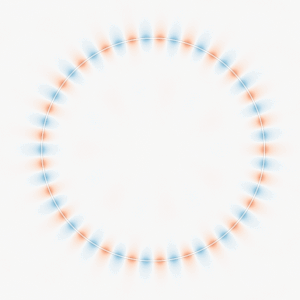
Finally, functionality in device application can be understood, for example by finite difference time domain simulation (FDTD using MEEP and python to do the animation) as shown above. Here, it is simulated how the electric field is confined inside a tube and a standing wave of a whispering gallery mode forms for near-IR radiation.
Semiconductor membranes as virtual substrates for epitaxy
We overgrow of freestanding semiconductor membranes to investigate the influence of these compliant substrates on the formation of self-assembled nanostructures (supported by FAPESP and CNPq). We are interested in understanding the growth dynamics during material deposition by molecular beam epitaxy. We investigate the surface diffusion by ex-situ methods like scanning electron microscopy and atomic force microscopy. Furthermore, we carry out x-ray diffraction to quantify the strain transfer from deposited material to the underlying substrate. Our goal is to demonstrate the possibilities of membranes as virtual substrate to tailor optical or electrical properties of heterostructures grown on top of them.
The image above depicts an AFM study of an overgrown, wrinkled InGaAs nanomembranes with InAs islands formed in the released areas of the sample (Nanotechnolgy 25, 455603 (2014)).
Growth of semiconductor hetero- and nanostructures
III-V heterostructures grown by molecular beam epitaxy are fundamental building blocks for research and technological applications. Being able to grow such structures requires a continuous development of the growth strategies to obtain structures with high optical or electrical quality.
Unstrained quantum dot structures

We have an ongoing research line for growing various kinds of III-V special tailored heterostructures for internal use or to provide for our collaborators. These include standard samples like GaAs quantum wells, InAs dots, and more advanced structures like Bragg reflectors or micro-cavity. Furthermore, we explore advanced heterostructures, and study – besides the membrane overgrowth – the fabrication of unstrained quantum emitters for optical applications or the fabrication of InAs flash dots for single photon sources.
The AFM images above depict structures made by Ga assisted deoxidation and local hole etching followed by the overgrowth with AlGaAs/GaAs/AlGaAs to develop unstrained mesoscopic GaAs structures (Nanoscale Research Letters 12, 61 (2017)).
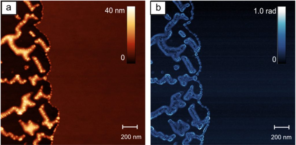
2D materials (graphene, hBN and TMDs)
Atomic thin 2D materials like graphene, hBN or transition metal dichalcogenide (TMDs) have gained tremendous attention in the last two decades. Their novel properties are explored in basic research as well as they are advertised as candidates for new electronic, opto-electronic, device such as solar cells or computation circuits.
In the past, I carried out basic studies of graphene, and I am interested in optical properties of TMDs and hBN. For example, we looked in to plasmons of graphene/hBN heterostructures using scattering scanning nearfield optical microscopy and couple infrared spectroscopy.
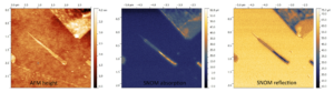
The image obtained with the Anasys AFMIR instrument of the LNNano shows the height image of a graphene flake as well as its reflection and absorption image using a CO2 laser as light source and the AFM tip as nano-antenna to probe the material. The contrast in the optical images arises from the formation of standing wave plasmons inside the graphene and confined by the nanometer size of the structure.
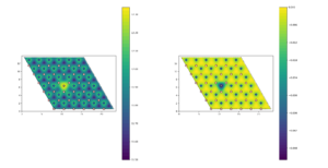
Density-functional theory (DFT) can be used to obtain new inside into these materials. The image above shows a calculated Scanning Tunneling Microscopy (STM) image using ASE and GPAW of a carbon defect inside a hBN matrix. Similar calculation could be used to describe and understand structural, electrical as well as optical properties of these materials. I have an increasing interest in carrying out such calculations with experimental data.

DOI: 10.1002/smll.202105424")

DOI: 10.1088/1361-6528/ac47ce")


DOI: 10.1088/1361-6528/ace4d1")

, 3140–3147 (2021)
DOI: 10.1021/acsanm.1c00354")

DOI: 10.1088/1361-6528/ab7d74")


