
Experimental physics courses are typically part of both Physics degree programmes and a wide range of engineering curricula. However, the objectives of these courses are often more closely associated with the verification of theoretical physics than with the practice of experimental physics itself or with an understanding of Physics as an experimental science and, therefore, as a discipline inherently connected to concepts such as measurement uncertainty and the incompleteness of models. In this article, we describe the implementation of a curricular reform in the introductory teaching laboratories of the Institute of Physics Gleb Wataghin at the University of Campinas (Unicamp). Through this reform, the focus of the courses shifted towards the development of skills relevant to experimental physics, rather than the reinforcement of theoretical physics. These skills were organised into three courses, comprising: (1) a minimum core of skills, such as performing and recording simple measurements; (2) basic skills, such as the calibration of instruments; and, finally, (3) the application of the acquired skills in project-based activities, aimed at fostering student autonomy. The experiments were selected to best highlight and develop each skill. This structure is presented in detail, and a proposal for its implementation is discussed, including examples of experiments for the three courses.
Luís E.E. de Araujo, Felippe A.S. Barbosa, Pierre-Louis de Assis, Sandro G. de Oliveira, Christoph Deneke, Guilherme S. Marcom, and Luiz Fernando Zagonel
Rev. Bras. Ensino Fís. 48 • 2026 DOI: 10.1590/1806-9126-RBEF-2025-0548
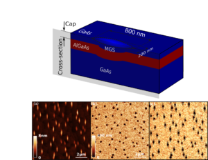
 Over the past two decades, epitaxial semiconductor quantum dots (QDs) have demonstrated very promising properties as sources of single and entangled photons on-demand. Among different growth methods, droplet etching epitaxy has allowed the growth of almost strain-free QDs, with low and controllable surface densities, small excitonic fine structure splitting (FSS), and fast radiative decays. Here, we extend the technique to In(Ga)As QDs in AlGaAs, thereby increasing the achievable emission wavelength range beyond that accessible to GaAs/AlGaAs QDs while preserving some of the key advantages of this growth method. We observe QD densities of ∼0.25 μm–2, FSS values as small as 3 μeV, and short radiative lifetimes of ∼300 ps, while extending the achievable emission wavelength to ∼900 nm at cryogenic temperatures. We envision these QDs to be particularly suitable for integrated quantum photonics applications.
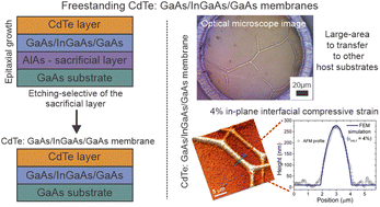 CdTe is a key binary compound for II-VI semiconductor systems since the precise control of its growth over different semiconductor materials of different orientations provides a general roadmap for telluride compounds, ranging from optically active layers to diluted magnetic semiconductors and topological insulators. The precise understanding of its epitaxy, film orientation and built-in strain is crucial for II-VI layer integration with commercial hosting substrates used for the latest semiconductor process nodes such as Si and GaAs. In this work, we show that it is feasible to use CdTe:GaAs/InGaAs/GaAs released membranes, yielding high-quality crystalline layers. A combination of Raman scattering and X-ray diffraction results provide a concise scenario of evolution along different growth stages. Surface roughness and contact potential are evaluated by atomic force and Kelvin-probe microscopy, respectively. The coexistence of faceting types (001) and (111) becomes clear using AFM and KPFM near the edge of a CdTe membrane. At such edges the local cleavage of the membrane is probed, exposing several layer steps and reflecting the growth history of CdTe. In this condition, KPFM clearly differentiates faceting (throughout contact potential difference) more accurately than height profiles, allowing a qualitative explanation of the nucleation evolution in our system. Finally, the occurrence of a 4% in-plane interfacial compressive strain is observed by nanomembrane release and modelling with finite element methods. The results showing the flexibility of high-quality CdTe layers here can improve optoelectronic integration of II-VI semiconductors.
 Our paper “Review: using rolled-up tubes for strain-tuning the optical properties of quantum emitters” is out.
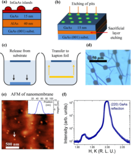
 Unstrained GaAs quantum dots are promising candidates for quantum information devices due to their optical properties, but their electronic properties have remained relatively unexplored until now. In this work, we systematically investigate the electronic structure and natural charging of GaAs quantum dots at room temperature using Kelvin probe force microscopy (KPFM). We observe a clear electrical signal from these structures demonstrating a lower surface potential in the middle of the dot. We ascribe this to charge accumulation and confinement inside these structures. Our systematical investigation reveals that the change in surface potential is larger for a nominal dot filling of 2 nm and then starts to decrease for thicker GaAs layers. Using k · p calculation, we show that the confinement comes from the band bending due to the surface Fermi level pinning. We find a correlation between the calculated charge density and the KPFM signal indicating that k · p calculations could be used to estimate the KPFM signal for a given structure. Our results suggest that these self-assembled structures could be used to study physical phenomena connected to charged quantum dots like Coulomb blockade or Kondo effect.
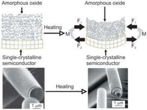 nanoscale assembly to access a broad range of 3D geometries and hybrid materials. An amorphous SrTiO3 layer on a Si:B/Si1−xGex:B heterostructure is reconfigured at the atomic scale upon heating, exhibiting a change in volume of ≈2% and accompanying biaxial stress. The Si:B/Si1−xGex:B bilayer is fabricated by molecular beam epitaxy, followed by sputter deposition of SrTiO3 at room temperature. The processes yield a hybrid oxide/semiconductor nanomembrane. Upon release from the substrate, the nanomembrane rolls up and has a curvature determined by the stress in the epitaxially grown Si:B/Si1−xGex:B heterostructure. Heating to 600 °C leads to a decrease of the radius of curvature consistent with the development of a large compressive biaxial stress during the reconfiguration of SrTiO3. The control of stresses via post-deposition processing provides a new route to the assembly of complex-oxide-based heterostructures in 3D geometry. The reconfiguration of metastable mechanical stressors enables i) synthesis of various types of strained superlattice structures that cannot be fabricated by direct growth and ii) technologies based on strain engineering of complex oxides via highly scalable lithographic processes and on large-area semiconductor substrates.
DOI: 10.1002/smll.202105424")

DOI: 10.1088/1361-6528/ac47ce")


DOI: 10.1088/1361-6528/ace4d1")

, 3140–3147 (2021)
DOI: 10.1021/acsanm.1c00354")

DOI: 10.1088/1361-6528/ab7d74")


