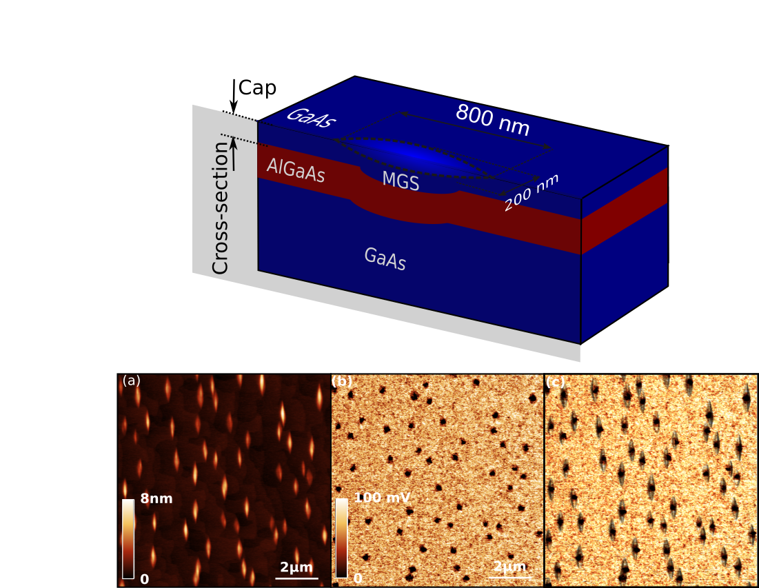
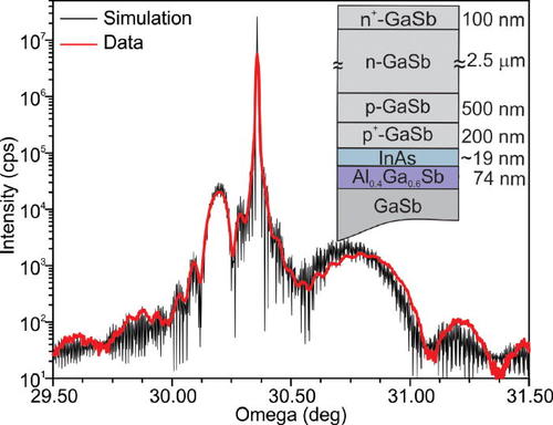
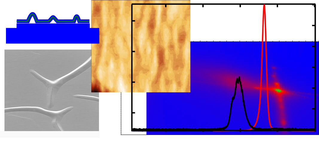
Our paper regarding the interference of electrical signals to MFM measurements is out. First publications with Unicamp as affiliation. Have a look at: “Separating the influence of electric charges in magnetic force microscopy images of inhomogeneous metal samples“.
Sep 15
Last images of Cassini
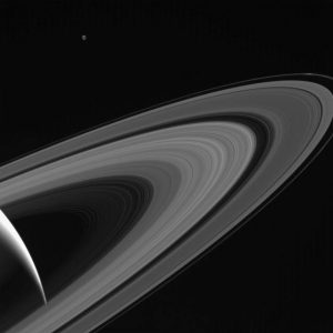 Today Friday, NASA let the probe Cassini enter into the atmosphere of Saturn, where it burned. The probe was delivering nice images and a lot of scientific data for 13 years.
Even so not nanotechnology, I always had a great interest in this kind of science as it teaches us a lot about the world, the solar system and about our selves.
Maybe, it shows again that some knowledge is important and of value beyond commercial use – something, we tend to forget in the times were everything seems to must have a “return of investment”.
Remember: All images of NASA (like the one on the side) are public domain and we can show them around and enjoy them.
Aug 22
FI199
Tomorrow will be the first round of FI199 – mainly repeating basic solid state physics and talking about semiconductor devices. Hope already to introduce the heterostructure that we can talk about epitaxy and epitaxial semiconductor nanostructures next week.
Aug 11
Conference week
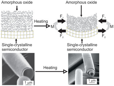
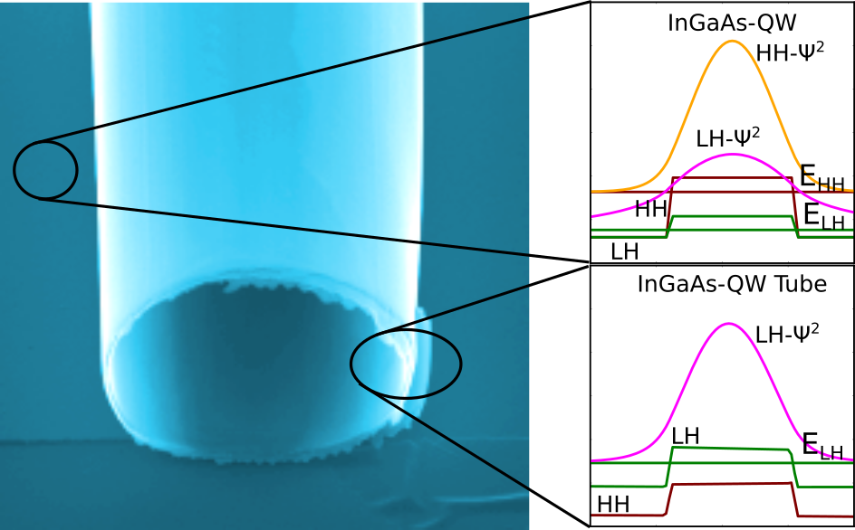
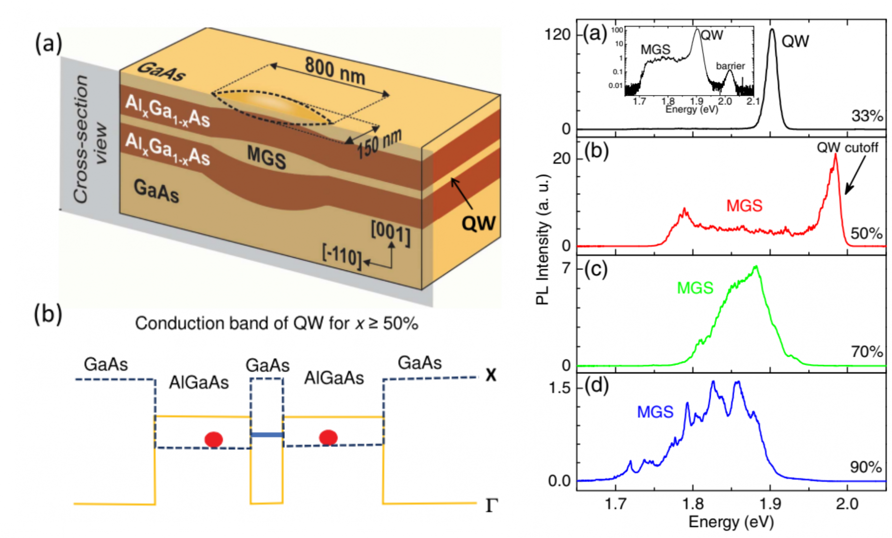
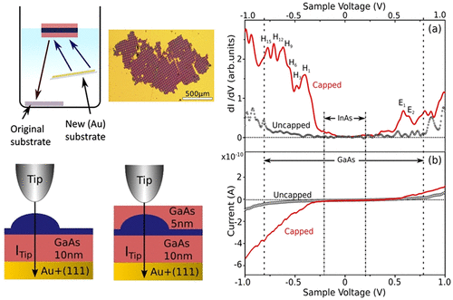
 BWSP is coming up – beside the MBE tutorial by myself, the are two talks related to our work: Ingrid will talk about our work on rolled-up tubes and Evandro will show our results on charging on unstrained mesoscopic GaAs structures.
See you there.
Aug 04
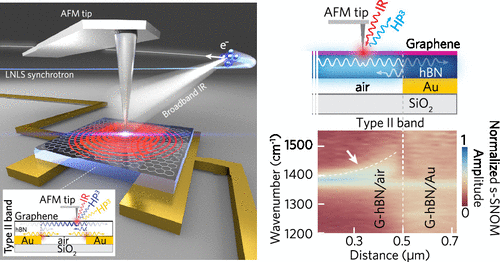
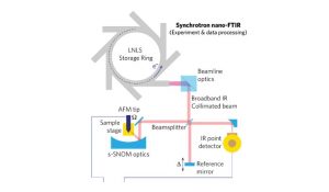
The IR beamline Synchrotron Radiation News article is out
The article describing the IR beamline of the LNLS is out. I was involved in setting up the experiments and also enjoyed in-house beamtime in the setup phase allowing to write our “Nanoscale” article on graphene/BN structures. Synchrotron Radiation News is coined towards the community and should give a nice advertising to the beamline.
Jul 28
Teaching 2nd semester 2017
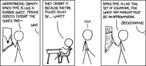
In my first semester at Unicamp, I will give F329 (Physics lab III) and contribute to FI199 with to lessons in August (Semiconductor nanostructures). Looking forward to do this. Hope, it will be better than in the xkcd strip below…
I will announce office ours next week.
Jul 14
Back making rolled-up tubes
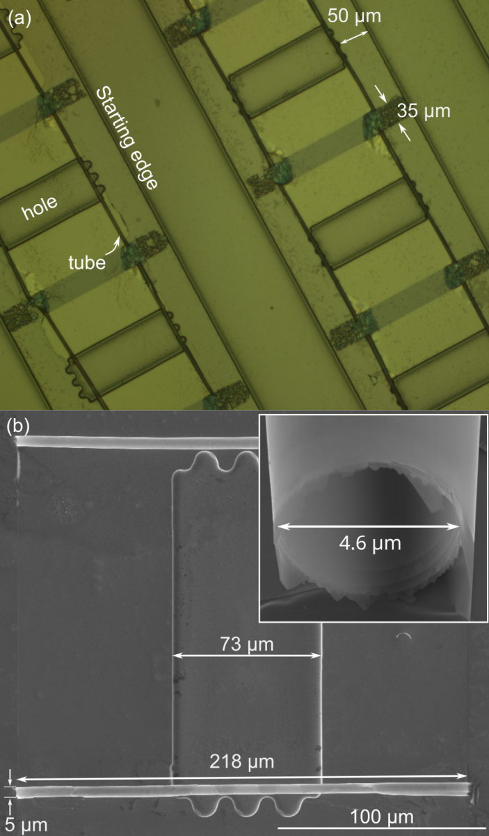
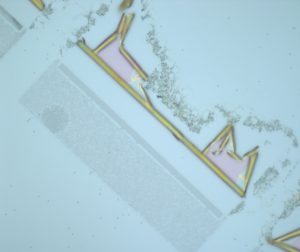 We are back to make rolled-up InGaAs/GaAs nano- and microtubes. We stopped doing the process for more than a year, but now is the time to strongly restart the activity.
The light microscopy image shows one of our first process. The MBE grown sample coming from our machine rolls nicely, but we have to optimize our process to place them on the sample surface and to control the roll-up.
In the past, this was not to hard and I hope, we be back to the excellent structures, we fabricated before, very soon.
These structures are related to our ongoing FAPESP project and we would always welcome another helping hand in the whole thing. We are still interested in doing hybrid radial superlattices and try to explore further functionality of the tubes.
Jul 07
AFM workshop at the LNNano
Scanning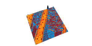 near field optical (SNOM) microscopy image of a graphene flak obtained during the AFM workshop at the LNNano using the NanoIR2-s system of the facility. We are back to the business of imaging garphene and restart this research line here as well as in collaboration with the CNPEM.
We had a lot of fun during the workshop and the chance to teach AFM and related techniques (I gave 9 times a course on EFM/KFM). Furthermore, a lot of interaction with the user of the AFM facilities, I am still in collaboration with, was happening showing that we have an active Brazilian AFM community. The image above shows, how important state of the art instrumentation is, but also which kind of nice images we can obtained in science.
Jun 29
Beware the impact factor
I just read an interesting interview in a German Online magazine with Noble prize winner Randy Schekman. He warns to out to much value into the impact factor of magazines like “Science” and “Nature” – indeed he claims, they not helping science to progress, but give rise to fashionable and not-solid research.
I agree with him: we have to come up with better systems to evaluate the quality, the importance and relevance of publications and science we do. I just have no idea, what is a better alternative at the current point.
Jun 23
II LNNano AFM Workshop
WE will have our II LNNano AFM Workshop from the 05. to the 07. July at the LNNano. We had a tremendous feedback to the event. I am looking forward to do the theoretical course and will administrate one of the practical parts of the Workshop.
The LCS group does a hard work making this happening.

