Luminescence in a Scanning Tunneling Microscope
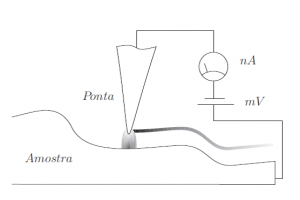
Scanning tunneling microscopy is a microscopy technique based on the tunneling effect. In this technique, an atomically sharp tip is brought close to a solid sample and by applying a potential difference between the sample and the tip, a tunneling current is generated between them. By moving the tip over the surface of the sample and keeping the tunneling current constant, it is possible to determine the topography of the sample with atomic resolution.
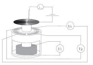
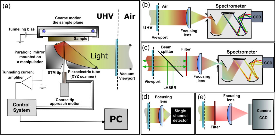
The tip movement is achieved by varying the voltage applied to piezoelectric crystals that are mounted, for example, on the base of the sample, as shown in the figure. Four crystals make the lateral movements (XY plane of the sample) and a fifth piezoelectric crystal makes the vertical movement. In this illustration, the tip remains fixed and the sample is moved.
Images can be obtained by varying the height of the sample (remembering that the tip is fixed) to maintain a constant distance between the tip apex and the sample surface. Thus, the movement of the sample can be used to reconstruct the surface topography. Depending on the conditions, it is possible to obtain images up to atomic resolution.
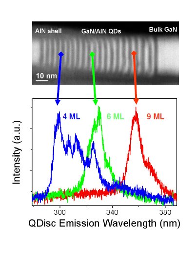
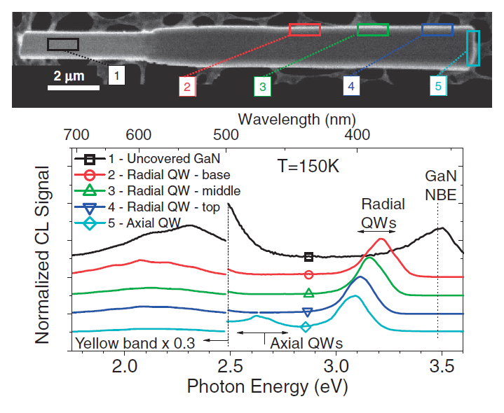
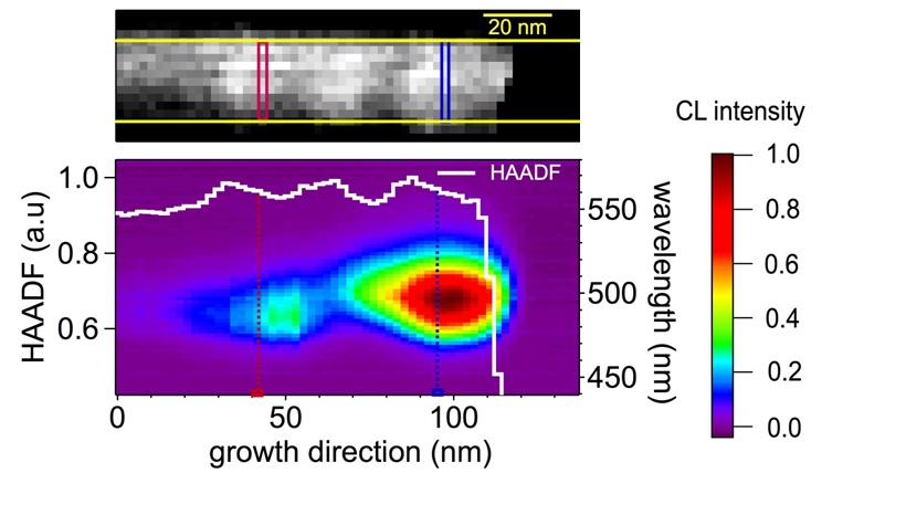
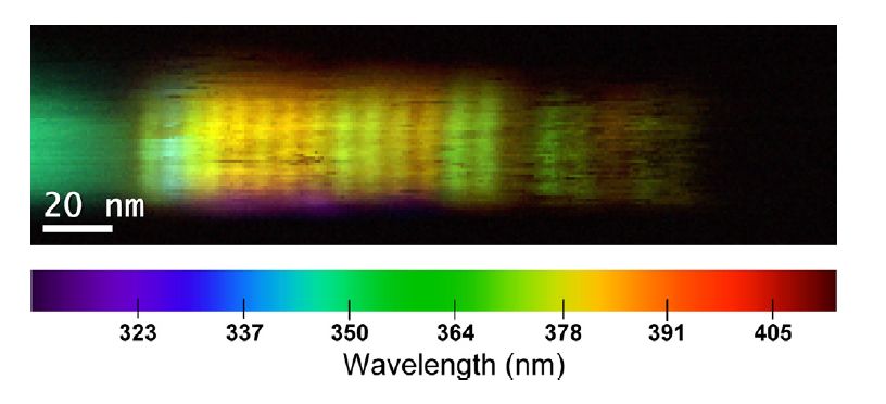
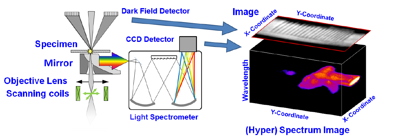
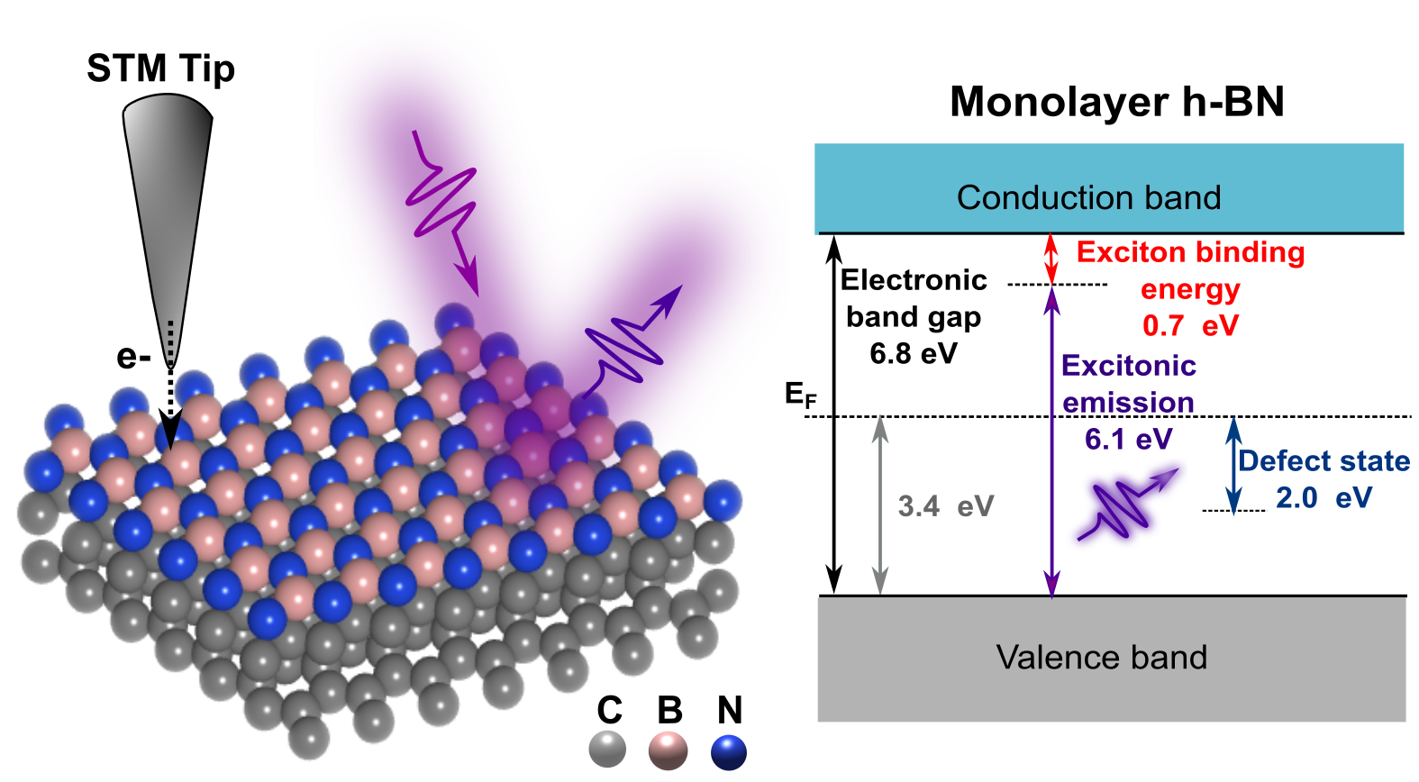
Furthermore, by adjusting the voltage between the tip and the sample, it is possible to inject charge carriers and generate local luminescence. By recovering the emitted light, it is possible to study the local luminescence spectrum of complex samples.
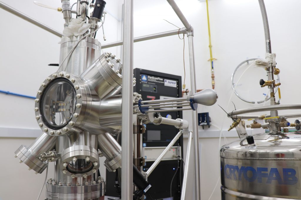
Photo of Scanning Tunneling Microscope (STM) operating in ultra high vacuum (UHV) and low temperatures (LT), reaching below 12 K.
Photos of the microscope inside the double shield that provides thermal insulation. On the right side there is a support with several samples and on the left side a support with several tips.
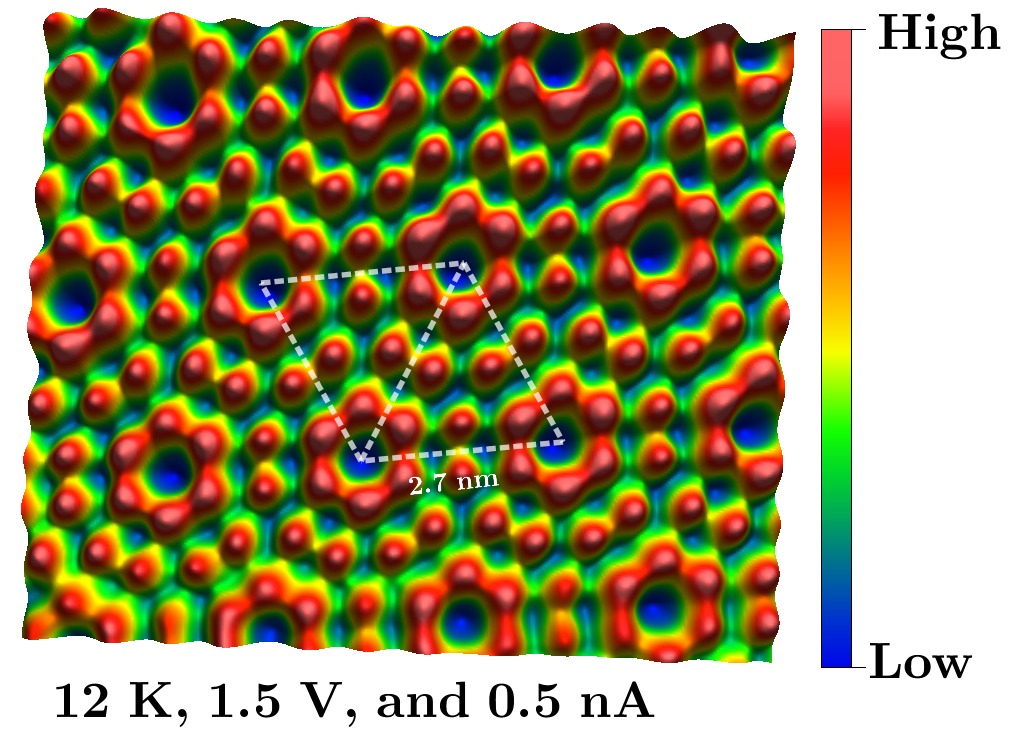
Image of the 7×7 reconstruction of the silicon 111 surface, observed at low temperature. The dark regions have lower relief than the lighter ones. Each round region in light tone corresponds to an individual atom.


