General Research Guidelines for Master’s/Doctorate/Post Doc Projects
Advisor: Luiz Fernando Zagonel (contact)
See more about the IFGW PhD Program here.
See more about the main equipment of this project (the STM) here.
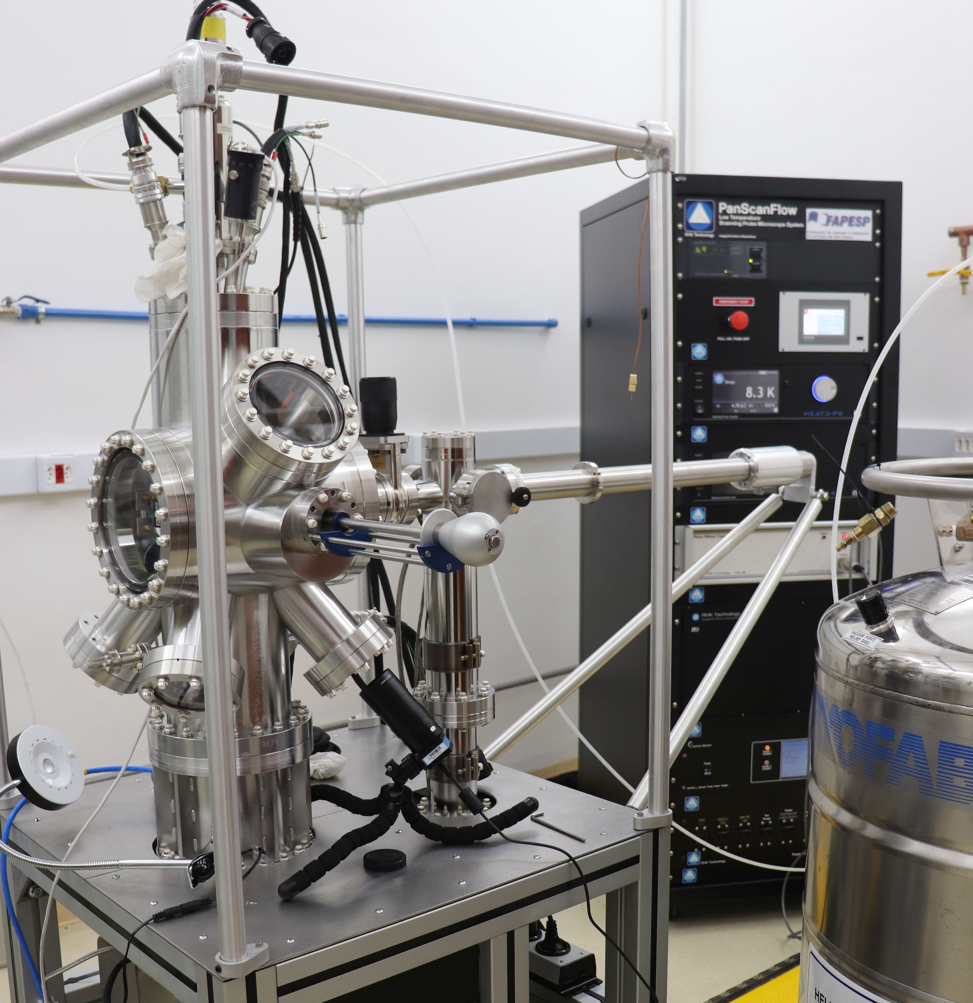
Figure: Photo of the Scanning Tunneling Microscope (STM) operating in UHV.
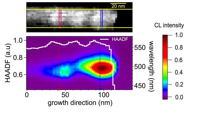
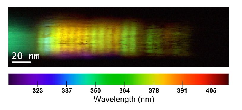
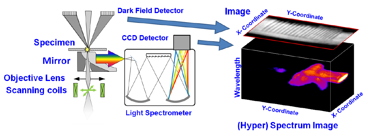
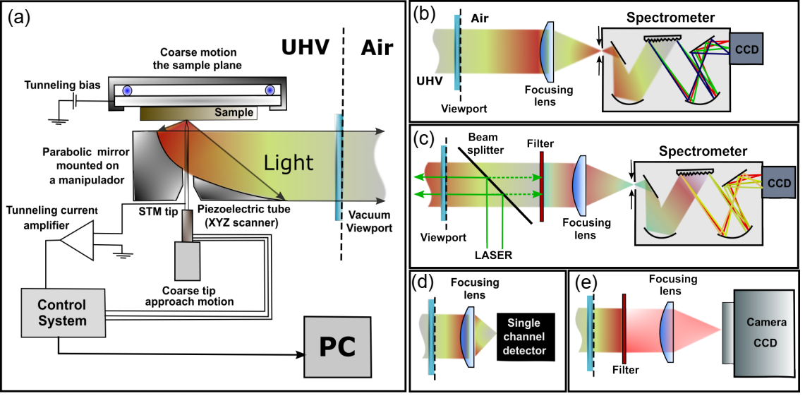
Our projects are focused on optical and electronic properties of optically active materials (absorbers and emitters) studied by Scanning Tunneling Microscopy (STM) associated with a high-performance optical device. This device, which was patented by our team, allows detecting the light emission induced by the tunneling current and also the injection of light near the STM tip. With this infrastructure, it is possible to study the morphology, electronic structure and light emission of individual nanostructures with high spatial and spectral resolution. The current focus of our group is on the interface between fundamental studies of advanced materials and studies of properties that may be relevant for technological applications (in particular in light emitters and absorbers).
In particular, we work with two-dimensional (2D) materials, h-BN and TMDs, and more recently with nanoparticles. We will be attentive to technologically relevant problems related to materials that have potential application as light emitters and absorbers in future devices, such as solar cells and light emitting diodes. These problems include the determination of band alignments and edges, substrate effects, defects, line broadening and others with a direct impact on device performance.
Our scanning tunneling microscope (pictured) has atomic resolution (that’s right, it is possible to observe individual atoms), operates at an Ultra-High-Vacuum pressure (about 1015 times lower than atmospheric pressure) and at cryogenic temperature (typically 15 Kelvins) through cooling with Liquid Helium. As if all this were not enough, it has a high-performance light detection system capable of collecting the light that the objects we are studying emit when the tunnel current passes through.
In these projects, we will use this instrument to study the light emitted by nano-structured materials and thus understand the optical properties of these materials in connection with their morphology.
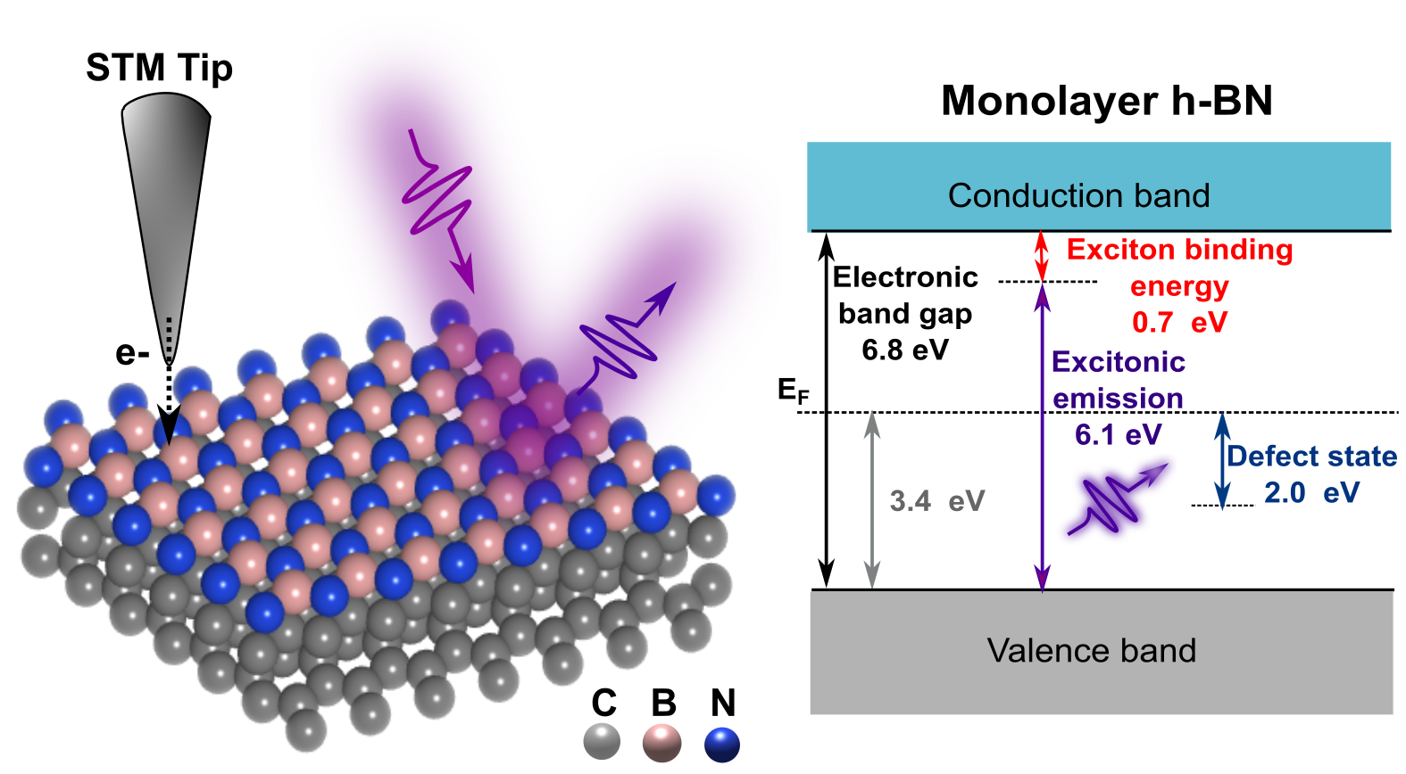
2D materials, such as h-BN and TMDs (WSe2, MoS2)
Two-dimensional materials when in a single monolayer present different properties than those commonly found when in many layers. A recent example is TMDs (transition metal dichalcogenides) which can even present a direct band gap and good quantum efficiency when in a monolayer. In fact, the search for new luminescent materials and, in particular, flexible materials has brought a lot of attention to TMDs and also to Boron Nitride.
In this research topic we want to study the light emission from these materials and observe defects and their luminescence. For this we will use luminescence induced by the tunnel current inside an STM (STML or STL). With this instrument we will have high spatial resolution, sufficient spectral resolution and the ability to inject carriers with different energies by adjusting the voltage between the tip and the sample. See one of the ongoing projects on this material. As a result already obtained in this project, above is an image with atomic resolution of the WSe2 surface together with a spectrum showing the valence and conduction bands.
Materials for solar cells (photovoltaic panels)
Sustainable energy production is an increasingly urgent challenge in modern society. In this line of research, we will study materials relevant to the manufacture of solar cells. In particular, our goal is to use the techniques available in our group (STM, STM and STM-LE) to better understand the role of each layer in solar cells based on perovskites and in particular how band alignment occurs within a solar cell based on these materials. In addition, we will study individual nanoparticles to understand how their inhomogeneity can compromise the properties of a solar cell based on such particles.
The samples will be prepared within our research group (Photovoltaic Research Laboratory) and also in collaborating groups (Nanotechnology and Solar Energy Laboratory – IQ-Unicamp).
Colloidal quantum wells
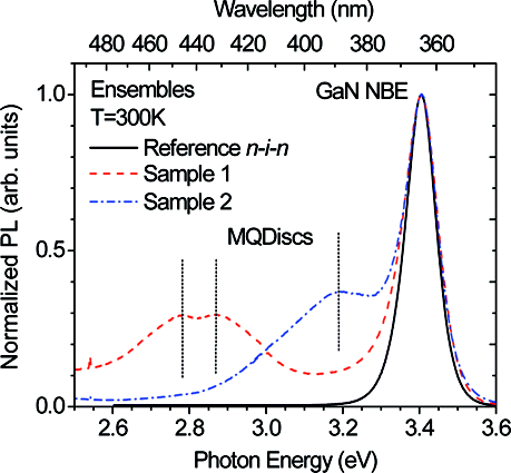
A widely used route in the synthesis of quantum wells is the manufacture through chemical precursors. In this case, the final producer is a solution with quantum wells in suspension. With this method, quantum wells of various materials can be fabricated, in particular quantum wells of III-V materials or perovskites. The interest here is the ability to study individual quantum wells and thus reveal differences between them and fine structures present in each one that are scrambled when sets are studied. See this recent article on this type of material.
As an example of results already obtained in this project, above are AFM and STM images of this sample indicating that a monolayer of it was generated by dispersion on a flat surface and also a photoluminescence spectrum obtained at room temperature.
Visit the system and talk about opportunities!


