For an updated list of publications, visit my ResearcherID Profile. Some manuscripts can be found on the Arxiv repository or on my personal web site. Below there is a list of selected publications.
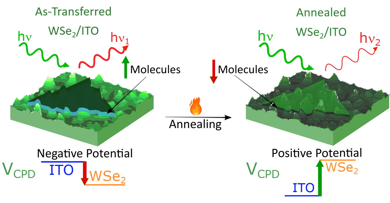
Investigating the impact of ITO substrates on the optical and electronic properties of WSe2 monolayers
Two-dimensional (2D) materials, particularly transition metal dichalcogenides (TMDs), have gathered significant attention due to their interesting electrical and optical properties. Among TMDs, monolayers of WSe2 exhibit a direct band gap and high exciton binding energy, which enhances photon emission and absorption even at room temperature. This study investigates the electronic and optical properties of WSe2 monolayers when they are mechanically transferred to indium tin oxide (ITO) substrates. ITO is a transparent conducting electrode (TCE) used in many industrial optoelectronic applications. Samples were mechanically transferred under ambient conditions, consequently trapping an adsorbate layer of atmospheric molecules unintentionally between the monolayer and the substrate. To reduce the amount of adsorbates, some samples were thermally annealed. Atomic force microscopy confirmed the presence of the adsorbate layer under the TMD and its partial removal after annealing. X-ray photoelectron spectroscopy confirmed the presence of carbon species among the adsorbates even after annealing. Photoluminescence measurements show that WSe2 remains optically active on ITO even after annealing. Moreover, the luminescence intensity and energy are affected by the amount of adsorbates under the WSe2 monolayer. Scanning tunnelling spectroscopy reveals that the TMD monolayer is n-doped, and that its band edges form a type I band alignment with ITO. Surface potential measurements show a polarity change after annealing, indicating that polar molecules, most likely water, are being removed. This comprehensive study shows that a TCE does not quench WSe2 luminescence even after a prolonged thermal annealing, although its optical and electronic properties are affected by unintentional adsorbates. These findings provide insights for better understanding, controlling, and design of 2D material heterostructures on TCEs. Link: https://iopscience.iop.org/article/10.1088/1361-6528/ad8fb4 Autores: Thiago G L Brito, Fábio J R Costa, Alisson Ceccatto, Charles A N de Almeida, Abner de Siervo, Odilon D D Couto Jr, Ingrid David Barcelos and Luiz Fernando Zagonel Citation: Thiago G L Brito et al 2025 Nanotechnology 36 055704.
|
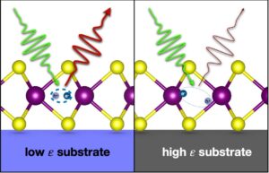
Impacts of dielectric screening on the luminescence of monolayer WSe2
Single layers of transition metal dichalcogenides, such as WSe2 have gaVersão ArXiv 2303.08957v1 thered increasing attention due to their intense electron-hole interactions, being considered promising candidates for developing novel optical applications. Within the few-layer regime, these systems become highly sensitive to the surrounding environment, enabling the possibility of using a proper substrate to tune desired aspects of these atomically-thin semiconductors. In this scenario, the dielectric environment provided by the substrates exerts significant influence on electronic and optical properties of these layered materials, affecting the electronic band-gap and the exciton binding energy. However, the corresponding effect on the luminescence of transition metal dichalcogenides is still under discussion. To elucidate these impacts, we used a broad set of materials as substrates for single-layers of WSe2, enabling the observation of these effects over a wide range of electrical permittivities. Our results demonstrate that an increasing permittivity induces a systematic red-shift of the optical band-gap of WSe2, intrinsically related to a considerable reduction of the luminescence intensity. Moreover, we annealed the samples to ensure a tight coupling between WSe2and its substrates, reducing the effect of undesired adsorbates trapped in the interface. Ultimately, our findings reveal how critical the annealing temperature can be, indicating that above a certain threshold, the heating treatment can induce adverse impacts on the luminescence. Furthermore, our conclusions highlight the influence the dielectric properties of the substrate have on the luminescence of WSe2, showing that a low electrical permittivity favours preserving the native properties of the adjacent monolayer. Authors: Fábio J R Costa, Thiago G-L Brito, Ingrid D Barcelos and Luiz Fernando Zagonel https://iopscience.iop.org/article/10.1088/1361-6528/acda3b Citation Fábio J R Costa et al 2023 Nanotechnology 34 385703 DOI 10.1088/1361-6528/acda3b
|
Design and implementation of a device based on an off-axis parabolic mirror to perform luminescence experiments in a scanning tunneling microscope
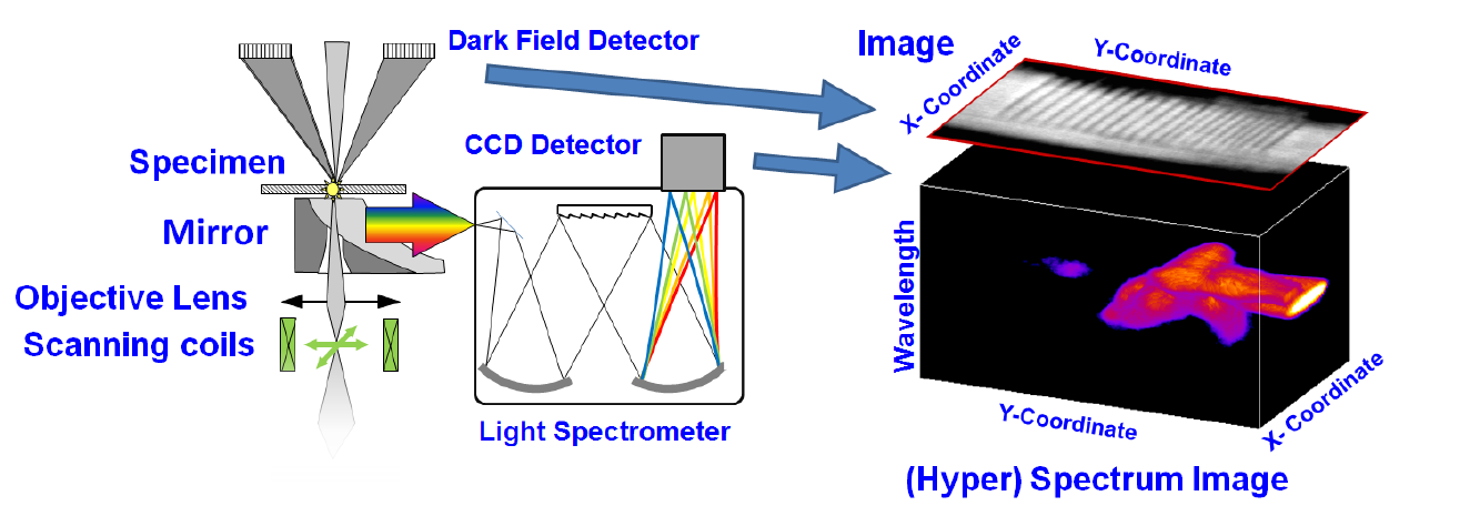
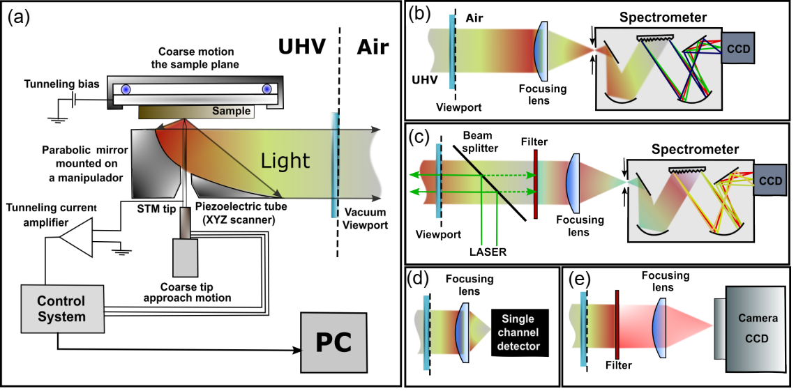
We present the design, implementation, and illustrative results of a light collection/injection strategy based on an off-axis parabolic mirror collector for a low-temperature Scanning Tunneling Microscope (STM). This device allows us to perform STM induced Light Emission (STM-LE) and Cathodoluminescence (STM-CL) experiments and in situ Photoluminescence (PL) and Raman spectroscopy as complementary techniques. Considering the Étendue conservation and using an off-axis parabolic mirror, it is possible to design a light collection and injection system that displays 72% of collection efficiency (considering the hemisphere above the sample surface) while maintaining high spectral resolution and minimizing signal loss. The performance of the STM is tested by atomically resolved images and scanning tunneling spectroscopy results on standard sample surfaces. The capabilities of our system are demonstrated by performing STM-LE on metallic surfaces and two-dimensional semiconducting samples, observing both plasmonic and excitonic emissions. In addition, we carried out in situ PL measurements on semiconducting monolayers and quantum dots and in situ Raman on graphite and hexagonal boron nitride (h-BN) samples. Additionally, STM-CL and PL were obtained on monolayer h-BN gathering luminescence spectra that are typically associated with intragap states related to carbon defects. The results show that the flexible and efficient light injection and collection device based on an off-axis parabolic mirror is a powerful tool to study several types of nanostructures with multiple spectroscopic techniques in correlation with their morphology at the atomic scale and electronic structure. https://aip.scitation.org/doi/abs/10.1063/5.0078423 Autores: Ricardo Javier Peña Román, Yves Auad, Lucas Grasso, Lazaro A Padilha, Fernando Alvarez, Ingrid David Barcelos, Mathieu Kociak, and Luiz Fernando Zagonel Citation: Ricardo Javier Peña Román et al Review of Scientific Instruments 93, 043704 (2022);
|
Band gap measurements of monolayer h-BN and insights into carbon-related point defects
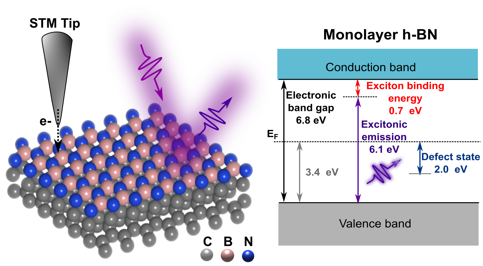
Being a flexible wide band gap semiconductor, hexagonal boron nitride (h-BN) has great potential for technological applications like efficient deep ultraviolet light sources, building block for two-dimensional heterostructures and room temperature single photon emitters in the ultraviolet and visible spectral range. To enable such applications, it is mandatory to reach a better understanding of the electronic and optical properties of h-BN and the impact of various structural defects. Despite the large efforts in the last years, aspects such as the electronic band gap value, the exciton binding energy and the effect of point defects remained elusive, particularly when considering a single monolayer. Here, we directly measured the density of states of a single monolayer of h-BN epitaxially grown on highly oriented pyrolytic graphite, by performing low temperature scanning tunneling microscopy (STM) and spectroscopy (STS). The observed h-BN electronic band gap on defect-free regions is (6.8 ± 0.2) eV. Using optical spectroscopy to obtain the h-BN optical band gap, the exciton binding energy is determined as being of (0.7 ± 0.2) eV. In addition, the locally excited cathodoluminescence and photoluminescence show complex spectra that are typically associated to intragap states related to carbon defects. Moreover, in some regions of the monolayer h-BN we identify, using STM, point defects which have intragap electronic levels around 2.0 eV below the Fermi level.
https://doi.org/10.1088/2053-1583/ac0d9c Roman, Ricardo Javier Pena; Costa, Fabio J. R. Costa; Zobelli, Alberto; Elias, Christine; Valvin, Pierre; Cassabois, Guillaume; Gil, Bernard; Summerfield, Alex; Cheng, Tin S.; Mellor, Christopher J.; Beton, Peter H.; Novikov, Sergei, V; Zagonel, Luiz F. Citation Ricardo Javier Peña Román et al 2021 2D Mater. 8 044001 |
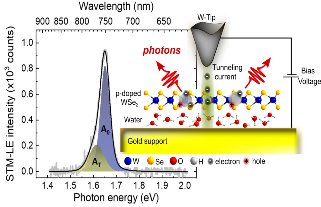
Tunneling-current-induced local excitonic luminescence in p-doped WSe2 monolayers
We have studied the excitonic properties of exfoliated tungsten diselenide (WSe2) monolayers transferred to gold substrates using the tunneling current in a Scanning Tunneling Microscope (STM) operated in air to excite the light emission locally. In obtained spectra, emission energies are independent of the applied bias voltage and resemble photoluminescence (PL) results, indicating that, in both cases, the light emission is due to neutral and charged exciton recombination. Interestingly, the electron injection rate, that is, the tunneling current, can be used to control the ratio of charged to neutral exciton emission. The obtained quantum yield in the transition metal dichalcogenide (TMD) is ∼5 × 10⁻⁷ photons per electron. The proposed excitation mechanism is the direct injection of carriers into the conduction band. The monolayer WSe2 presents bright and dark defects spotted by STM images performed under UHV. STS confirms the sample as p-doped, possibly as a net result of the observed defects. The presence of an interfacial water layer decouples the monolayer from the gold support and allows excitonic emission from the WSe2 monolayer. The creation of a water layer is an inherent feature of the sample transferring process due to the ubiquitous air moisture. Consequently, vacuum thermal annealing, which removes the water layer, quenches excitonic luminescence from the TMD. The tunneling current can locally displace water molecules leading to excitonic emission quenching and to plasmonic emission due to the gold substrate. The present findings extend the use and the understanding of STM induced light emission (STM-LE) on semiconducting TMDs to probe exciton emission and dynamics with high spatial resolution.
https://doi.org/10.1039/D0NR03400B Ricardo Javier Peña Román, Yves Auad, Lucas Grasso, Fernando Alvarez, Ingrid David Barcelos and Luiz Fernando Zagonel Nanoscale, 2020,12, 13460-13470. |
|
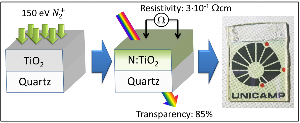
This study reports on the properties of nitrogen doped titanium dioxide (TiO2) thin films considering the application as transparent conducting oxide (TCO). Sets of thin films were prepared by sputtering a titanium target under oxygen atmosphere on a quartz substrate at 400 or 500°C. Films were then doped at the same temperature by 150 eV nitrogen ions. The films were prepared in Anatase phase which was maintained after doping. Up to 30at% nitrogen concentration was obtained at the surface, as determined by in situ x-ray photoelectron spectroscopy (XPS). Such high nitrogen concentration at the surface lead to nitrogen diffusion into the bulk which reached about 25 nm. Hall measurements indicate that average carrier density reached over 1019 cm-3 with mobility in the range of 0.1 to 1 cm2V-1s-1. Resistivity about 3.10-1 Wcm could be obtained with 85% light transmission at 550 nm. These results indicate that low energy implantation is an effective technique for TiO2 doping that allows an accurate control of the doping process independently from the TiO2 preparation. Moreover, this doping route seems promising to attain high doping levels without significantly affecting the film structure. Such approach could be relevant for preparation of N:TiO2 transparent conduction electrodes (TCE). https://doi.org/10.1016/j.apsusc.2018.02.259 Raul Ramos, Diego Scoca, Rafael Borges Merlo, Francisco Chagas Marques, Fernando Alvarez, Luiz Fernando Zagonel* Journal: Applied Surface Science, Volume 443, 2018, Pages 619-627.
|
Nanometer-scale monitoring of quantum-confined Stark effect and emission efficiency droop in multiple GaN/AlN quantum disks in nanowires
|
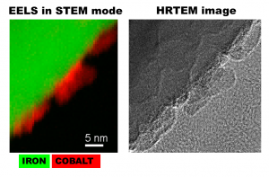
Photocatalytic hydrogen production of Co(OH)2 nanoparticle-coated α-Fe2O3 nanoringsReference: Nanoscale, 2013,5, 9310-9316. Authors: Heberton Wender, Renato V. Gonçalves, Carlos Sato B. Dias, Maximiliano J. M. Zapata, Luiz F. Zagonel, Edielma C. Mendonça, Sérgio R. Teixeira and Flávio Garcia |
Seeing and measuring in colours: Electron microscopy and spectroscopies applied to nano-optics |
Nanometer Scale Spectral Imaging of Quantum Emitters in Nanowires and Its Correlation to Their Atomically Resolved Structure |
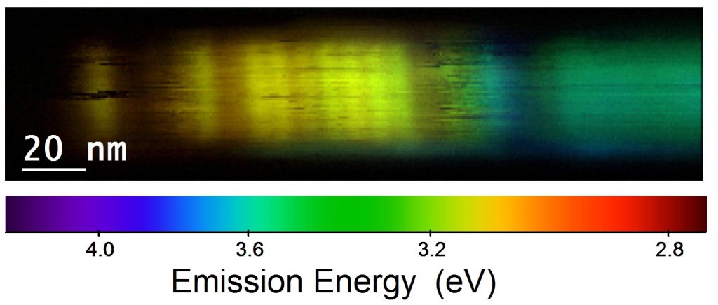
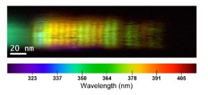
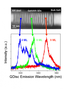
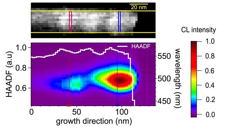
Visualising highly localised luminescence in GaN/AlN heterostructures in nanowiresThe optical properties of a stack of GaN/AlN quantum discs (QDiscs) in a GaN nanowire have been studied by spatially resolved cathodoluminescence (CL) at the nanoscale (nanoCL) using a Scanning Transmission Electron Microscope (STEM) operating in spectrum imaging mode. For the electron beam excitation in the QDisc region, the luminescence signal is highly localized with spatial extension as low as 5 nm due to the high band gap difference between GaN and AlN. This allows for the discrimination between the emission of neighbouring QDiscs and for evidencing the presence of lateral inclusions, about 3 nm thick and 20 nm long rods (quantum rods, QRods), grown unintentionally on the nanowire sidewalls. These structures, also observed by STEM dark-field imaging, are proven to be optically active in nanoCL, emitting at similar, but usually shorter, wavelengths with respect to most QDiscs. Rerence: Nanotechnology 23 (2012) 455205. Authors: L. F. Zagonel, L. Rigutti, M. Tchernycheva, G. Jacopin, R. Songmuang, M. Kociak
|
Growth mechanism and properties of InGaN insertions in GaN nanowires
We demonstrate the strong influence of strain on the morphology and In content of InGaN insertions in GaN nanowires, in agreement with theoretical predictions which establish that InGaN island nucleation on GaN nanowires may be energetically favorable, depending on In content and nanowire diameter. EDX analyses reveal In inhomogeneities between the successive dots but also along the growth direction within each dot, which is attributed to compositional pulling. Nanometer-resolved cathodoluminescence on single nanowires allowed us to probe the luminescence of single dots, revealing enhanced luminescence from the high In content top part with respect to the lower In content dot base.
Reference: Nanotechnology 23 (2012) 135703 (6pp).
Authors: G Tourbot, C Bougerol, F Glas, L F Zagonel, Z Mahfoud, S Meuret, P Gilet, M Kociak, B Gayraland and B Daudin.
|
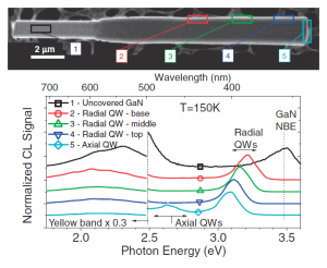
Single-Wire Light-Emitting Diodes Based on GaN Wires Containing Both Polar and Nonpolar InGaN/GaN Quantum Wells
Single-wire light-emitting diodes based on radial p–i–n multi quantum well (QW) junctions have been realized from GaN wires grown by catalyst-free metal organic vapor phase epitaxy. The Inx Ga1Àx N/GaN undoped QW system is coated over both the nonpolar lateral sidewalls and on the polar upper surface. Cathodo- and electroluminescence (EL) experiments provide evidence that the polar QWs emit in the visible spectral range at systematically lower energy than the nonpolar QWs. The EL of the polar or nonpolar QWs can be selectively activated by varying the sample temperature and current injection level. Reference: Applied Physics Express 5 (2012) 014101. Authors: Gwenole Jacopin, Andre De Luna Bugallo, Pierre Lavenus, Lorenzo Rigutti, Francois H. Julien, Luiz F. Zagonel, Mathieu Kociak, Christophe Durand, Damien Salomon, Xiao Jun Chen, Joel Eymery, and Maria Tchernycheva.
|
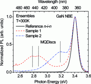
Ultraviolet Photodetector Based on GaN/AlN Quantum Disks in a Single Nanowire
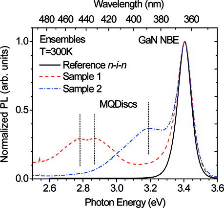
We report the demonstration of single-nanowire photodetectors relying on carrier generation in GaN/AlN QDiscs. Two nanowire samples containing QDiscs of different thicknesses are analyzed and compared to a reference binary n-i-n GaN nanowire sample. The responsivity of a single wire QDisc detector is as high as 2 × 10 3 A/W at λ ) 300 nm at room temperature. We show that the insertion of an axial heterostructure drastically reduces the dark current with respect to the binary nanowires and enhances the photosensitivity factor (i.e., the ratio between the photocurrent and the dark current) up to 5 × 10 2 for an incoming light intensity of 5 mW/cm2. Photocurrent spectroscopy allows identifcation of the spectral contribution related to carriers generated within large QDiscs, which lies below the GaN band gap due to the quantum confined Stark effect. Reference: Nano Letters 2010, 10, 2939. Authors: L. Rigutti, M. Tchernycheva, A. De Luna Bugallo, G. Jacopin, F. H. Julien, L. F. Zagonel, K. March, O. Stephan, M. Kociak, and R. Songmuang
|
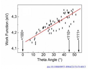
Orientation-dependent work function of in situ annealed strontium titanate (SrTiO3)
We have used energy-filtered x-ray photoelectron emission microscopy (XPEEM) and synchrotron radiation to measure the grain orientation dependence of the work function of a sintered niobium-doped strontium titanate (SrTiO3) ceramic. A significant spread in work function values is found. Grain orientation and surface reducing/oxidizing conditions are the main factors in determining the work function. Energy-filtered XPEEM looks ideally suited for analysis of other technologically interesting polycrystalline samples. The mean work function value is 4.26 eV with a standard deviation of 0.06 eV. The grain orientation is determined by electron backscattered diffraction and correlated with the XPEEM work functions. A good linear correlation is obtained between WF and the polar EBSD angle θ . In particular, the work functions determined for the three principal crystal faces [100], [110] and [111] are 4.13, 4.32 and 4.34 eV, respectively. Reference: J. Phys.: Condens. Matter 21 (2009) 314013. |
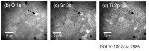
Orientation-dependent surface composition ofin situ annealed strontium titanate
The surface composition of polycrystalline niobium-doped strontium titanate (SrTiO3: Nb) is studied using X-ray photoelectron emission microscopy (XPEEM) for many grain orientations in order to characterise the surface chemistry with high spatial resolution. The surface sensitivity is maximised by the use of soft X-ray synchrotron radiation (SR). The grain orientation is determined by electron backscattering diffraction (EBSD). Stereographic plots are used to show the correlation between surface composition and orientation for several grains. Predominant surface terminations are assigned to major orientations.Reference: Surface and Interface Analysis 2008, 40, 1709–1712. |
Full field chemical imaging of buried native sub-oxide layers on doped silicon patterns
Fully energy-filtered X-ray photoelectron emission microscopy is used to analyze the spatial distribution of the silicon sub-oxide structure at the SiO2/Si interface as a function of underlying doping pattern. Using a spectroscopic pixel-by-pixel curve fitting analysis, we obtain the sub-oxide binding energy and intensity distributions over the full field of view. Binding energy maps for each oxidation state are obtained with a spatial resolution of 120 nm. Within the framework of a five-layer model, the experimental data are used to obtain quantitative maps of the sub-oxide layer thickness and also their spatial distribution over the p–n junctions. Variations in the sub-oxide thicknesses are found to be linked to the level and type of doping. The procedure, which takes into account instrumental artefacts, enables the quantitative analysis of the full 3D dataset. Reference: Surface Science 604 (2010) 1628–1636 DOI: 10.1016/j.susc.2010.06.006
|
Effect of Carbon on the Compound Layer Properties of AISI H13 Tool Steel in Pulsed Plasma Nitrocarburizing
Due to the mechanical and inertness properties of the e-Fe2-3N phase, its formation as a compact monolayer is most wanted in plasma surface treatments of steels. This phase can be obtained by the inclusion of carbon species in the plasma. In this work, we present a systematic study of the carbon influence on the compound layer in an AISI H13 tool steel by pulsed plasma nitrocarburizing process with different gaseous ratios (0% =< [CH4]/[N2+CH4+H2] =< 4%). The plasma treatment was carried out for 5 h at 575 °C. The microstructure and phase composition of the modified layers were studied by scanning electron microscopy and X-ray diffraction, respectively. X-Ray photoelectron spectroscopy was used to measure the relative concentration of carbon and nitrogen on the surface. The hardening profile induced by the nitrocarburized process is also reported. Reference: Plasma Process. Polym. 2007, 4, S728–S731. |


