
I finished reading a very good philosophy book trying to figure out, what makes science in its way to acquire knowledge different from other approaches. “The Scientific Attitude: Defending Science from Denial, Fraud, and Pseudoscience” by Lee McIntyre is interesting making the point the difference is not the method, but the attitude how evidence is gathered and used to progress the knowledge of the world. He tells us that this attitude separates scientist from non-scientiest and lead to the strength of the scientific obtained understanding of the world making it special against all other knowledge.
Whereas I like the idea to separate the scientific endeavor by its attitude and values involved rather then by a scientific method, I have to admit, his science idea is to much an empirical one influenced by logical positivism, Popper and Kuhn. I personally see a strong component that acquiring of knowledge and therefor also science has its base in empirical phenomena, but also a synthesis part as pointed out by Kant. In some way, McIntyre might agree with this as he points out that science not only reports the empirical finding, but the knowledge must come with a warrant.
Also it is interesting to see, how Galileo Galilei is mentioned to be a victim of the science believe of his time. There should be mentioned: No one believed in this time that the earth is flat – the solar system just was assumed to be heliocentric; the catholic church is not really the science community – Galileo’s science colleagues of the time like Copernicus (who suggested the heliocentric defended by Galileo Galilei), Johannes Kepler and Tycho Brahe already gave up on the geocentric world idea – it were people outside the sciences that did not want to believe this.
Anyway, the book is very interesting and I enjoyed reading it. I can just recommend it for people doing science as well as people not doing science. It is an important contribution in these times, where scientific knowledge is seen as a opinion among others and forgotten that generations of scientist worked to arrive on the current point of knowledge. Therefore, the current state of scientific knowledge contains the experience of many tries (and failures) to understand the world. If the knowledge is gathered with the right, scientific attitude, it is our best chance to be the correct one.
P.S.: Peer review is not as good as hoped in the book and the important fact checking is done afterwards by the community; and scientific progress does not happened in Paradigmatic shifts, but in a hard creeping way of small continuous steps (sometimes with some impressive jumps from people at the right time and place, which would not possible, if the previous generations of scientist had not collected all the data).
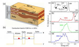 We investigate the optical properties of strain-free mesoscopic GaAs/Al(x)Ga(1-x)As structures (MGS) coupled to thin GaAs/A(x)Ga(1-x)As quantum wells (QWs) with varying Al content (x). We demonstrate that quenching the QW emission by controlling the band crossover between AlGaAs X-point and GaAs Gamma-point gives rise to long carrier lifetimes and enhanced optical emission from the MGS. For x = 0.33, QW and MGS show typical type-I band alignment with strong QW photoluminescence emission and much weaker sharp recombination lines from the MGS localized exciton states. For x >= 0.50, the QW emission is considerably quenched due to the change from type-I to type-II structure while the MGS emission is enhanced due to carrier injection from the QW. For x >= 0.70, we observe PL quenching from the MGS higher energy states also due to the crossover of X and Gamma bands, demonstrating spectral filtering of the MGS emission. Time-resolved measurements reveal two recombination processes in the MGS emission dynamics. The fast component depends mainly on the X-Gamma mixing of the MGS states and can be increased from 0.3 to 2.5~ns by changing the Al content. The slower component, however, depends on the X-Gamma mixing of the QW states and is associated to the carrier injection rate from the QW reservoir into the MGS structure. In this way, the independent tuning of X-Gamma mixing in QW and MGS states allows us to manipulate recombination rates in the MGS as well as to make carrier injection and light extraction more efficient.
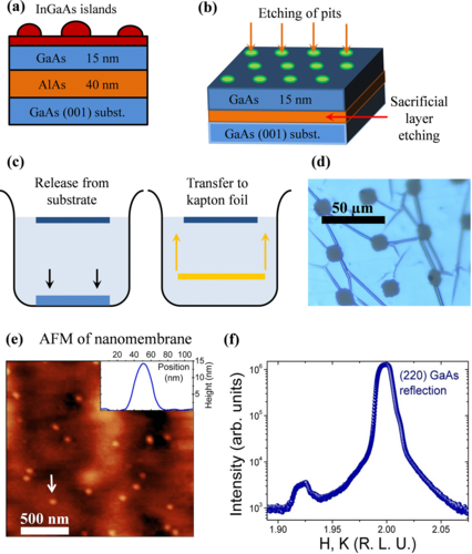
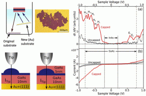 Nanoscale heterostructure engineering is the main target for the development of optoelectronic devices. In this sense, a precise knowledge of local electronic response after materials processing is required to envisage technological applications. A number of local probe techniques that address single nanostructure signals were satisfactorily employed in semiconductor epitaxial systems. In this work we show that the use of chemically etched semiconductor nanomembranes allows carrying out scanning tunneling spectroscopy (STS) measurements in a postprocessed system which was otherwise studied mainly under in situ conditions that differ from the operational regime. We were able to acquire STS spectra with energy level resolved response on InAs quantum dots grown within a 15 nm-thick GaAs single-crystalline film transferred to an Au(111) surface. The presence of a native oxide layer does not affect the result, keeping the reliability of the usual ultra high vacuum (UHV) procedures. The use of nanomembranes also opens up the possibility of tailoring properties via additional variables such as nanomembrane thickness and surface charge depletion. Our method is applicable to a broad class of postprocessed layers extracted in nanomembrane format from epitaxial systems that are potential candidates for optoelectronic applications.
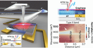 n of free-space radiation at sub-wavelength scales. Most notably, the van der Waals heterostructure composed of graphene (G) and hexagonal boron nitride (hBN) provides for gate-tunable hybrid hyperbolic plasmon phonon-polaritons (HP3). Here, we present the anisotropic flow control and gate-voltage modulation of HP3 modes in G-hBN on an air–Au microstructured substrate. Using broadband infrared synchrotron radiation coupled to a scattering-type near-field optical microscope, we launch HP3 waves in both hBN Reststrahlen bands and observe directional propagation across in-plane heterointerfaces created at the air–Au junction. The HP3 hybridization is modulated by varying the gate voltage between graphene and Au. This modifies the coupling of continuum graphene plasmons with the discrete hBN hyperbolic phonon polaritons, which is described by an extended Fano model. This work represents the first demonstration of the control of polariton propagation, introducing a theoretical approach to describe the breaking of the reflection and transmission symmetry for HP3 modes. Our findings augment the degree of control of polaritons in G-hBN and related hyperbolic metamaterial nanostructures, bringing new opportunities for on-chip nano-optics communication and computing.
 fundamental challenge in heteroepitaxy. On-demand transfer of light-emitting structures to arbitrary host substrates is an important technological path for optoelectronics and photonics devices implementation. The use of freestanding membranes as compliant substrates is a promising approach to address both issues.
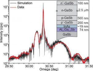 We demonstrate thin-film GaSb solar cells which are isolated from a GaSb substrate and transferred to a Si substrate. We epitaxially grow ∼3.3 μm thick GaSb P on N diode structures on a GaSb substrate. Upon patterning in 2D arrays of pixels, the GaSb films are released via epitaxial lift-off and they are transferred to Si substrates. Encapsulation of each pixel preserves the structural integrity of the GaSb film during lift-off. Using this technique, we consistently transfer ∼4 × 4 mm2 array of pixelated GaSb membranes to a Si substrate with a ∼ 80%–100% yield. The area of individual pixels ranges from ∼90 × 90 μm2 to ∼340 × 340 μm2. Further processing to fabricate photovoltaic devices is performed after the transfer. GaSb solar cells with lateral sizes of ∼340 × 340 μm2 under illumination exhibit efficiencies of ∼3%, which compares favorably with extracted values for large-area (i.e., 5 × 5 mm2) homoepitaxial GaSb solar cells on GaSb substrates.

DOI: 10.1002/smll.202105424")

DOI: 10.1088/1361-6528/ac47ce")


DOI: 10.1088/1361-6528/ace4d1")

, 3140–3147 (2021)
DOI: 10.1021/acsanm.1c00354")

DOI: 10.1088/1361-6528/ab7d74")


