
Sandhya; Manimunda Susarla, Praveena; Morais Jaques
Deformation Mechanisms of Vertically Stacked WS2 /MoS2 Heterostructures: The Role of Interfaces Journal Article
In: ACS Nano, vol. 12, no. 4, pp. 4036−4044, 2018.
@article{Susarla2018,
title = {Deformation Mechanisms of Vertically Stacked WS2 /MoS2 Heterostructures: The Role of Interfaces},
author = {Susarla, Sandhya; Manimunda, Praveena; Morais Jaques, Ygor; Hachtel, Jordan; Idrobo, Juan Carlos; Syed Amanulla, Syed Asif; Galvao, Douglas; Tiwary, Chandra; Ajayan, Pulickel},
url = {https://pubs.acs.org/doi/10.1021/acsnano.8b01786},
doi = {DOI: 10.1021/acsnano.8b01786},
year = {2018},
date = {2018-04-05},
journal = {ACS Nano},
volume = {12},
number = {4},
pages = {4036−4044},
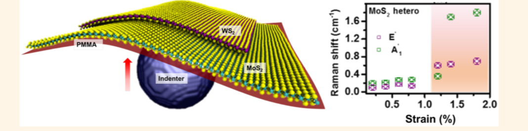
abstract = {The mechanical and optical properties generated due to the stacking of different atomically thin materials
have made it possible to tune and engineer these materials for next-generation electronics. The understanding of the
interlayer interactions in such stacked structures is of fundamental interest for structure and property correlation. Here, a
combined approach of in situ Raman spectroscopy and mechanical straining along with molecular dynamics (MD)
simulations has been used to probe one such interface, namely, the WS2/MoS2 heterostructure. Vertical heterostructures on
poly(methyl methacrylate), when flexed, showed signs of decoupling at 1.2% strain. Theoretical calculations showed straininduced
stacking changes at 1.75% strain. The sliding characteristics of layers were also investigated using scanning probe
microscopy based nanoscratch testing, and the results are further supported by MD simulations. The present study could
be used to design future optoelectronic devices based on WS2/MoS2 heterostructures.},
keywords = {},
pubstate = {published},
tppubtype = {article}
}
have made it possible to tune and engineer these materials for next-generation electronics. The understanding of the
interlayer interactions in such stacked structures is of fundamental interest for structure and property correlation. Here, a
combined approach of in situ Raman spectroscopy and mechanical straining along with molecular dynamics (MD)
simulations has been used to probe one such interface, namely, the WS2/MoS2 heterostructure. Vertical heterostructures on
poly(methyl methacrylate), when flexed, showed signs of decoupling at 1.2% strain. Theoretical calculations showed straininduced
stacking changes at 1.75% strain. The sliding characteristics of layers were also investigated using scanning probe
microscopy based nanoscratch testing, and the results are further supported by MD simulations. The present study could
be used to design future optoelectronic devices based on WS2/MoS2 heterostructures.
Jaques, Y. M.; Manimunda, P.; Nakanishi, Y.; Susarla, S.; Woellner, C. F.; Bhowmick, S.; Asif, S. A. S.; Galvao, D. S.; Tiwary, C. S.; Ajayan, P. M.
Differences in the Mechanical Properties of Monolayer and Multilayer WSe2/MoSe2 Journal Article
In: MRS Advances, vol. 3, no. 6-7, pp. 373-378, 2018.
@article{Jaques2018,

title = {Differences in the Mechanical Properties of Monolayer and Multilayer WSe2/MoSe2},

author = {Y. M. Jaques and P. Manimunda and Y. Nakanishi and S. Susarla and C. F. Woellner and S. Bhowmick and S. A. S. Asif and D. S. Galvao and C. S. Tiwary and P. M. Ajayan},

url = {https://www.cambridge.org/core/journals/mrs-advances/article/differences-in-the-mechanical-properties-of-monolayer-and-multilayer-wse2mose2/4F6AFF52BCE7DFFF87E35AC424A8F0BE},

doi = { https://doi.org/10.1557/adv.2018.246},

year  = {2018},

date = {2018-03-01},

journal = {MRS Advances},

volume = {3},

number = {6-7},

pages = {373-378},

abstract = {Transition metal dichalcogenides are 2D structures with remarkable electronic, chemical, optical and mechanical properties. Monolayer and crystal properties of these structures have been extensively investigated, but a detailed understanding of the properties of their few-layer structures are still missing. In this work we investigated the mechanical differences between monolayer and multilayer WSe2 and MoSe2, through fully atomistic molecular dynamics simulations (MD). It was observed that single layer WSe2/MoSe2 deposited on silicon substrates have larger friction coefficients than 2, 3 and 4 layered structures. For all considered cases it is always easier to peel off and/or to fracture MoSe2 structures. These results suggest that the interactions between first layer and substrate are stronger than interlayer interactions themselves. Similar findings have been reported for other nanomaterials and it has been speculated whether this is a universal-like behavior for 2D layered materials. We have also analyzed fracture patterns. Our results show that fracture is chirality dependent with crack propagation preferentially perpendicular to W(Mo)-Se bonds and faster for zig-zag-like defects.},

keywords = {},

pubstate = {published},

tppubtype = {article}

}
Jaques, Y. M.; Manimunda, P.; Nakanishi, Y.; Susarla, S.; Woellner, C. F.; Bhowmick, S.; Asif, S. A. S.; Galvao, D. S.; C. S. Tiwary,; Ajayan, P. M.
Differences in the Mechanical Properties of Monolayer and Multilayer WSe2/MoSe2 Online
2018, (preprint arXiv:1801.05641).
@online{Jaques2018b,

title = {Differences in the Mechanical Properties of Monolayer and Multilayer WSe2/MoSe2},

author = {Y. M. Jaques and P. Manimunda and Y. Nakanishi and S. Susarla and C. F. Woellner and S. Bhowmick and S. A. S. Asif and D. S. Galvao and C. S. Tiwary, and P. M. Ajayan},

url = {https://arxiv.org/abs/1801.05641},

year  = {2018},

date = {2018-01-18},

abstract = {Transition metal dichalcogenides are 2D structures with remarkable electronic, chemical, optical and mechanical properties. Monolayer and crystal properties of these structures have been extensively investigated, but a detailed understanding of the properties of their few-layer structures are still missing. In this work we investigated the mechanical differences between monolayer and multilayer WSe2 and MoSe2, through fully atomistic molecular dynamics simulations (MD). It was observed that single layer WSe2/MoSe2 deposited on silicon substrates have larger friction coefficients than 2, 3 and 4 layered structures. For all considered cases it is always easier to peel off and/or to fracture MoSe2 structures. These results suggest that the interactions between first layer and substrate are stronger than interlayer interactions themselves. Similar findings have been reported for other nanomaterials and it has been speculated whether this is a universal-like behavior for 2D layered materials. We have also analyzed fracture patterns. Our results show that fracture is chirality dependent with crack propagation preferentially perpendicular to W(Mo)-Se bonds and faster for zig-zag-like defects.},

note = {preprint arXiv:1801.05641},

keywords = {},

pubstate = {published},

tppubtype = {online}

}
Manimunda, P; Nakanishi, Y; Jaques, YM; Susarla, S; Woellner, CF; Bhowmick, S; Asif, SAS; Galvao, DS; Tiwary, CS; Ajayan, PM
Nanoscale deformation and friction characteristics of atomically thin WSe2 and heterostructure using nanoscratch and Raman spectroscopy Journal Article
In: 2D Materials, vol. 4, no. 4, pp. 045005, 2017.
@article{Manimunda2017,

title = {Nanoscale deformation and friction characteristics of atomically thin WSe2 and heterostructure using nanoscratch and Raman spectroscopy},

author = {Manimunda, P and Nakanishi, Y and Jaques, YM and Susarla, S and Woellner, CF and Bhowmick, S and Asif, SAS and Galvao, DS and Tiwary, CS and Ajayan, PM},

url = {http://iopscience.iop.org/article/10.1088/2053-1583/aa8475/meta},

doi = {10.1088/2053-1583/aa8475},

year  = {2017},

date = {2017-08-23},

journal = {2D Materials},

volume = {4},

number = {4},

pages = {045005},

abstract = {2D transition metals di-selenides are attracting a lot of attention due to their interesting optical, chemical and electronics properties. Here, the deformation characteristics of monolayer, multi- layer WSe2 and its heterostructure with MoSe2 were investigated using a new technique that combines nanoscratch and Raman spectroscopy. The 2D monolayer WSe2 showed anisotropy in deformation. Effect of number of WSe2 layers on friction characteristics were explored in detail. Experimental observations were further supported by MD simulations. Raman spectra recorded from the scratched regions showed strain induced degeneracy splitting. Further nano-scale scratch tests were extended to MoSe2–WSe2 lateral heterostructures. Effect of deformation on lateral hetero junctions were further analysed using PL and Raman spectroscopy. This new technique is completely general and can be applied to study other 2D materials.},

keywords = {},

pubstate = {published},

tppubtype = {article}

}
Chandra Sekhar Tiwary Sujin P Jose, Suppanat Kosolwattana
Enhanced supercapacitor performance of a 3D architecture tailored using atomically thin rGO–MoS 2 2D sheets Journal Article
In: RSC Advances, vol. 6, pp. 93384-93393, 2016.
@article{Jose2016,
title = {Enhanced supercapacitor performance of a 3D architecture tailored using atomically thin rGO–MoS 2 2D sheets},
author = {Sujin P Jose, Chandra Sekhar Tiwary, Suppanat Kosolwattana, Prasanth Raghavan, Leonardo D Machado, Chandkiram Gautam, T Prasankumar, Jarin Joyner, Sehmus Ozden, Douglas S Galvao, PM Ajayan},
url = {xlink.rsc.org/?DOI=c6ra20960b},
doi = {10.1039/C6RA20960B},
year = {2016},
date = {2016-09-19},
journal = {RSC Advances},
volume = {6},
pages = {93384-93393},
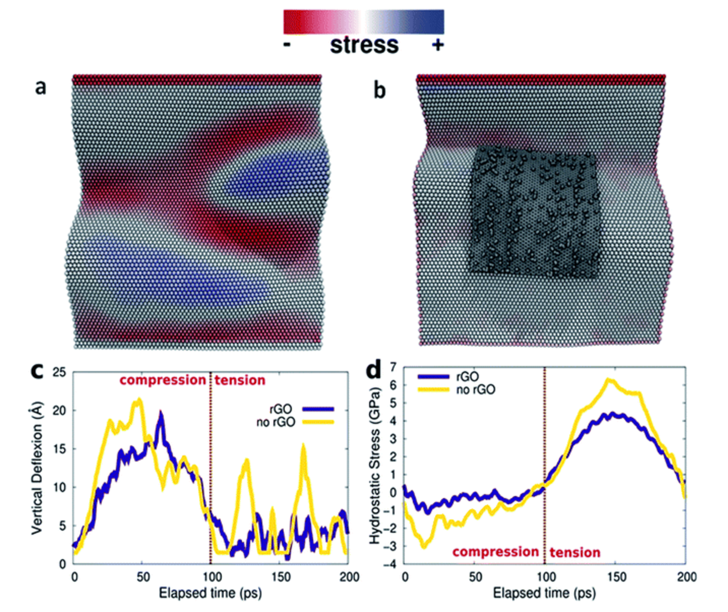
abstract = {A 3D architecture is fabricated using 2D nano-sheets of GO and MoS2 as the building blocks by a facile, one-pot chronoamperometry method to achieve a conductive additive free, binder free and scalable supercapacitor electrode. The superior electrochemical properties of the 3D PPy-rGO–MoS2 (PGMo) are due to its porous structure, thin wall, high surface area and high electrical conductivity that endow rapid transportation of electrolyte ions and electrons throughout the electrode matrix. The synergistic effect between the components in a proper ratio improves the supercapacitor performance and material stability of PGMo. The possible correlation of the structure and electrochemical performance of the 3D ternary composite is backed by a fully atomistic molecular dynamics (MD) simulation study. The high specific capacitance (387 F g−1) and impressive cycling stability (>1000 cycles) estimated for PGMo open up an opportunity to consider the 3D ternary nanostructures as cutting edge materials for energy storage solutions.
},
keywords = {},
pubstate = {published},
tppubtype = {article}
}
Yongji Gong Bo Li, Zhili Hu
Solid–Vapor Reaction Growth of Transition‐Metal Dichalcogenide Monolayers Journal Article
In: Angewandte Chemie, vol. 128, no. 36, pp. 10814-10819, 2016.
@article{Li2016,
title = {Solid–Vapor Reaction Growth of Transition‐Metal Dichalcogenide Monolayers},
author = {Bo Li, Yongji Gong, Zhili Hu, Gustavo Brunetto, Yingchao Yang, Gonglan Ye, Zhuhua Zhang, Sidong Lei, Zehua Jin, Elisabeth Bianco, Xiang Zhang, Weipeng Wang, Jun Lou, Douglas S Galvão, Ming Tang, Boris I Yakobson, Robert Vajtai, Pulickel M Ajayan},
url = {onlinelibrary.wiley.com/doi/10.1002/anie.201604445/abstract},
doi = {10.1002/ange.201604445},
year = {2016},
date = {2016-08-26},
journal = {Angewandte Chemie},
volume = {128},
number = {36},
pages = {10814-10819},
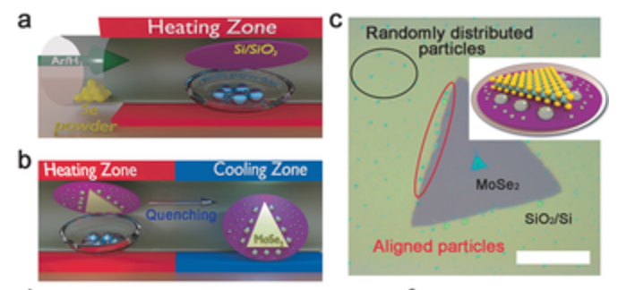
abstract = {Two-dimensional (2D) layered semiconducting transition-metal dichalcogenides (TMDCs) are promising candidates for next-generation ultrathin, flexible, and transparent electronics. Chemical vapor deposition (CVD) is a promising method for their controllable, scalable synthesis but the growth mechanism is poorly understood. Herein, we present systematic studies to understand the CVD growth mechanism of monolayer MoSe2, showing reaction pathways for growth from solid and vapor precursors. Examination of metastable nanoparticles deposited on the substrate during growth shows intermediate growth stages and conversion of non-stoichiometric nanoparticles into stoichiometric 2D MoSe2 monolayers. The growth steps involve the evaporation and reduction of MoO3 solid precursors to sub-oxides and stepwise reactions with Se vapor to finally form MoSe2. The experimental results and proposed model were corroborated by ab initio Car–Parrinello molecular dynamics studies.},
keywords = {},
pubstate = {published},
tppubtype = {article}
}
Xifan Wang Sidong Lei, Bo Li
Surface functionalization of two-dimensional metal chalcogenides by Lewis acid–base chemistry Journal Article
In: Nature Nanotechnology, vol. 11, pp. 465–471, 2016.
@article{Lei2016,
title = {Surface functionalization of two-dimensional metal chalcogenides by Lewis acid–base chemistry},
author = {Sidong Lei, Xifan Wang, Bo Li, Jiahao Kang, Yongmin He, Antony George, Liehui Ge, Yongji Gong, Pei Dong, Zehua Jin, Gustavo Brunetto, Weibing Chen, Zuan-Tao Lin, Robert Baines, Douglas S. Galvão, Jun Lou, Enrique Barrera, Kaustav Banerjee, Robert Vajtai & Pulickel Ajayan},
url = {http://www.nature.com/nnano/journal/vaop/ncurrent/full/nnano.2015.323.html},
doi = {10.1038/nnano.2015.323},
year = {2016},
date = {2016-02-01},
journal = {Nature Nanotechnology},
volume = {11},
pages = {465–471},
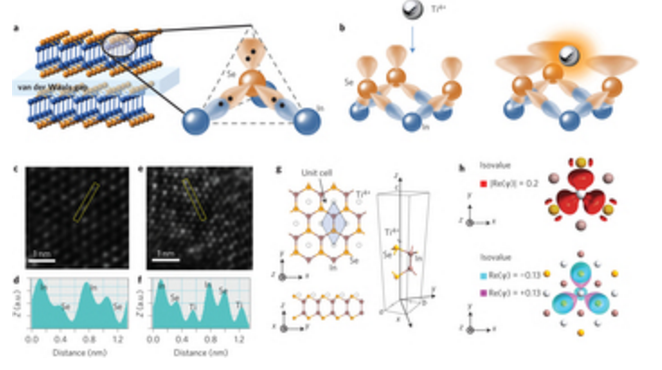
abstract = {Precise control of the electronic surface states of two-dimensional (2D) materials could improve their versatility and widen their applicability in electronics and sensing. To this end, chemical surface functionalization has been used to adjust the electronic properties of 2D materials. So far, however, chemical functionalization has relied on lattice defects and physisorption methods that inevitably modify the topological characteristics of the atomic layers. Here we make use of the lone pair electrons found in most of 2D metal chalcogenides and report a functionalization method via a Lewis acid–base reaction that does not alter the host structure. Atomic layers of n-type InSe react with Ti4+ to form planar p-type [Ti4+n(InSe)] coordination complexes. Using this strategy, we fabricate planar p–n junctions on 2D InSe with improved rectification and photovoltaic properties, without requiring heterostructure growth procedures or device fabrication processes. We also show that this functionalization approach works with other Lewis acids (such as B3+, Al3+ and Sn4+) and can be applied to other 2D materials (for example MoS2, MoSe2). Finally, we show that it is possible to use Lewis acid–base chemistry as a bridge to connect molecules to 2D atomic layers and fabricate a proof-of-principle dye-sensitized photosensing device.
},
keywords = {},
pubstate = {published},
tppubtype = {article}
}
2018
Sandhya; Manimunda Susarla, Praveena; Morais Jaques
Deformation Mechanisms of Vertically Stacked WS2 /MoS2 Heterostructures: The Role of Interfaces Journal Article
In: ACS Nano, vol. 12, no. 4, pp. 4036−4044, 2018.
Abstract | Links | BibTeX | Tags: Chalcogenides, Modeling
@article{Susarla2018,

title = {Deformation Mechanisms of Vertically Stacked WS2 /MoS2 Heterostructures: The Role of Interfaces},

author = {Susarla, Sandhya; Manimunda, Praveena; Morais Jaques, Ygor; Hachtel, Jordan; Idrobo, Juan Carlos; Syed Amanulla, Syed Asif; Galvao, Douglas; Tiwary, Chandra; Ajayan, Pulickel},

url = {https://pubs.acs.org/doi/10.1021/acsnano.8b01786},

doi = {DOI: 10.1021/acsnano.8b01786},

year  = {2018},

date = {2018-04-05},

journal = {ACS Nano},

volume = {12},

number = {4},

pages = {4036−4044},

abstract = {The mechanical and optical properties generated due to the stacking of different atomically thin materials

have made it possible to tune and engineer these materials for next-generation electronics. The understanding of the

interlayer interactions in such stacked structures is of fundamental interest for structure and property correlation. Here, a

combined approach of in situ Raman spectroscopy and mechanical straining along with molecular dynamics (MD)

simulations has been used to probe one such interface, namely, the WS2/MoS2 heterostructure. Vertical heterostructures on

poly(methyl methacrylate), when flexed, showed signs of decoupling at 1.2% strain. Theoretical calculations showed straininduced

stacking changes at 1.75% strain. The sliding characteristics of layers were also investigated using scanning probe

microscopy based nanoscratch testing, and the results are further supported by MD simulations. The present study could

be used to design future optoelectronic devices based on WS2/MoS2 heterostructures.},

keywords = {Chalcogenides, Modeling},

pubstate = {published},

tppubtype = {article}

}
have made it possible to tune and engineer these materials for next-generation electronics. The understanding of the
interlayer interactions in such stacked structures is of fundamental interest for structure and property correlation. Here, a
combined approach of in situ Raman spectroscopy and mechanical straining along with molecular dynamics (MD)
simulations has been used to probe one such interface, namely, the WS2/MoS2 heterostructure. Vertical heterostructures on
poly(methyl methacrylate), when flexed, showed signs of decoupling at 1.2% strain. Theoretical calculations showed straininduced
stacking changes at 1.75% strain. The sliding characteristics of layers were also investigated using scanning probe
microscopy based nanoscratch testing, and the results are further supported by MD simulations. The present study could
be used to design future optoelectronic devices based on WS2/MoS2 heterostructures.
Jaques, Y. M.; Manimunda, P.; Nakanishi, Y.; Susarla, S.; Woellner, C. F.; Bhowmick, S.; Asif, S. A. S.; Galvao, D. S.; Tiwary, C. S.; Ajayan, P. M.
Differences in the Mechanical Properties of Monolayer and Multilayer WSe2/MoSe2 Journal Article
In: MRS Advances, vol. 3, no. 6-7, pp. 373-378, 2018.
Abstract | Links | BibTeX | Tags: Chalcogenides, Modeling
@article{Jaques2018,

title = {Differences in the Mechanical Properties of Monolayer and Multilayer WSe2/MoSe2},

author = {Y. M. Jaques and P. Manimunda and Y. Nakanishi and S. Susarla and C. F. Woellner and S. Bhowmick and S. A. S. Asif and D. S. Galvao and C. S. Tiwary and P. M. Ajayan},

url = {https://www.cambridge.org/core/journals/mrs-advances/article/differences-in-the-mechanical-properties-of-monolayer-and-multilayer-wse2mose2/4F6AFF52BCE7DFFF87E35AC424A8F0BE},

doi = { https://doi.org/10.1557/adv.2018.246},

year  = {2018},

date = {2018-03-01},

journal = {MRS Advances},

volume = {3},

number = {6-7},

pages = {373-378},

abstract = {Transition metal dichalcogenides are 2D structures with remarkable electronic, chemical, optical and mechanical properties. Monolayer and crystal properties of these structures have been extensively investigated, but a detailed understanding of the properties of their few-layer structures are still missing. In this work we investigated the mechanical differences between monolayer and multilayer WSe2 and MoSe2, through fully atomistic molecular dynamics simulations (MD). It was observed that single layer WSe2/MoSe2 deposited on silicon substrates have larger friction coefficients than 2, 3 and 4 layered structures. For all considered cases it is always easier to peel off and/or to fracture MoSe2 structures. These results suggest that the interactions between first layer and substrate are stronger than interlayer interactions themselves. Similar findings have been reported for other nanomaterials and it has been speculated whether this is a universal-like behavior for 2D layered materials. We have also analyzed fracture patterns. Our results show that fracture is chirality dependent with crack propagation preferentially perpendicular to W(Mo)-Se bonds and faster for zig-zag-like defects.},

keywords = {Chalcogenides, Modeling},

pubstate = {published},

tppubtype = {article}

}
Jaques, Y. M.; Manimunda, P.; Nakanishi, Y.; Susarla, S.; Woellner, C. F.; Bhowmick, S.; Asif, S. A. S.; Galvao, D. S.; C. S. Tiwary,; Ajayan, P. M.
Differences in the Mechanical Properties of Monolayer and Multilayer WSe2/MoSe2 Online
2018, (preprint arXiv:1801.05641).
Abstract | Links | BibTeX | Tags: Chalcogenides, Mechanical Properties, Modeling
@online{Jaques2018b,

title = {Differences in the Mechanical Properties of Monolayer and Multilayer WSe2/MoSe2},

author = {Y. M. Jaques and P. Manimunda and Y. Nakanishi and S. Susarla and C. F. Woellner and S. Bhowmick and S. A. S. Asif and D. S. Galvao and C. S. Tiwary, and P. M. Ajayan},

url = {https://arxiv.org/abs/1801.05641},

year  = {2018},

date = {2018-01-18},

abstract = {Transition metal dichalcogenides are 2D structures with remarkable electronic, chemical, optical and mechanical properties. Monolayer and crystal properties of these structures have been extensively investigated, but a detailed understanding of the properties of their few-layer structures are still missing. In this work we investigated the mechanical differences between monolayer and multilayer WSe2 and MoSe2, through fully atomistic molecular dynamics simulations (MD). It was observed that single layer WSe2/MoSe2 deposited on silicon substrates have larger friction coefficients than 2, 3 and 4 layered structures. For all considered cases it is always easier to peel off and/or to fracture MoSe2 structures. These results suggest that the interactions between first layer and substrate are stronger than interlayer interactions themselves. Similar findings have been reported for other nanomaterials and it has been speculated whether this is a universal-like behavior for 2D layered materials. We have also analyzed fracture patterns. Our results show that fracture is chirality dependent with crack propagation preferentially perpendicular to W(Mo)-Se bonds and faster for zig-zag-like defects.},

note = {preprint arXiv:1801.05641},

keywords = {Chalcogenides, Mechanical Properties, Modeling},

pubstate = {published},

tppubtype = {online}

}
2017
Manimunda, P; Nakanishi, Y; Jaques, YM; Susarla, S; Woellner, CF; Bhowmick, S; Asif, SAS; Galvao, DS; Tiwary, CS; Ajayan, PM
Nanoscale deformation and friction characteristics of atomically thin WSe2 and heterostructure using nanoscratch and Raman spectroscopy Journal Article
In: 2D Materials, vol. 4, no. 4, pp. 045005, 2017.
Abstract | Links | BibTeX | Tags: Chalcogenides, Heterostructures, Molecular Dynamics
@article{Manimunda2017,

title = {Nanoscale deformation and friction characteristics of atomically thin WSe2 and heterostructure using nanoscratch and Raman spectroscopy},

author = {Manimunda, P and Nakanishi, Y and Jaques, YM and Susarla, S and Woellner, CF and Bhowmick, S and Asif, SAS and Galvao, DS and Tiwary, CS and Ajayan, PM},

url = {http://iopscience.iop.org/article/10.1088/2053-1583/aa8475/meta},

doi = {10.1088/2053-1583/aa8475},

year  = {2017},

date = {2017-08-23},

journal = {2D Materials},

volume = {4},

number = {4},

pages = {045005},

abstract = {2D transition metals di-selenides are attracting a lot of attention due to their interesting optical, chemical and electronics properties. Here, the deformation characteristics of monolayer, multi- layer WSe2 and its heterostructure with MoSe2 were investigated using a new technique that combines nanoscratch and Raman spectroscopy. The 2D monolayer WSe2 showed anisotropy in deformation. Effect of number of WSe2 layers on friction characteristics were explored in detail. Experimental observations were further supported by MD simulations. Raman spectra recorded from the scratched regions showed strain induced degeneracy splitting. Further nano-scale scratch tests were extended to MoSe2–WSe2 lateral heterostructures. Effect of deformation on lateral hetero junctions were further analysed using PL and Raman spectroscopy. This new technique is completely general and can be applied to study other 2D materials.},

keywords = {Chalcogenides, Heterostructures, Molecular Dynamics},

pubstate = {published},

tppubtype = {article}

}
2016
Chandra Sekhar Tiwary Sujin P Jose, Suppanat Kosolwattana
Enhanced supercapacitor performance of a 3D architecture tailored using atomically thin rGO–MoS 2 2D sheets Journal Article
In: RSC Advances, vol. 6, pp. 93384-93393, 2016.
Abstract | Links | BibTeX | Tags: Chalcogenides, DFT, graphene oxide, Molecular Dynamics
@article{Jose2016,

title = {Enhanced supercapacitor performance of a 3D architecture tailored using atomically thin rGO–MoS 2 2D sheets},

author = {Sujin P Jose, Chandra Sekhar Tiwary, Suppanat Kosolwattana, Prasanth Raghavan, Leonardo D Machado, Chandkiram Gautam, T Prasankumar, Jarin Joyner, Sehmus Ozden, Douglas S Galvao, PM Ajayan},

url = {xlink.rsc.org/?DOI=c6ra20960b},

doi = {10.1039/C6RA20960B},

year  = {2016},

date = {2016-09-19},

journal = {RSC Advances},

volume = {6},

pages = {93384-93393},

abstract = {A 3D architecture is fabricated using 2D nano-sheets of GO and MoS2 as the building blocks by a facile, one-pot chronoamperometry method to achieve a conductive additive free, binder free and scalable supercapacitor electrode. The superior electrochemical properties of the 3D PPy-rGO–MoS2 (PGMo) are due to its porous structure, thin wall, high surface area and high electrical conductivity that endow rapid transportation of electrolyte ions and electrons throughout the electrode matrix. The synergistic effect between the components in a proper ratio improves the supercapacitor performance and material stability of PGMo. The possible correlation of the structure and electrochemical performance of the 3D ternary composite is backed by a fully atomistic molecular dynamics (MD) simulation study. The high specific capacitance (387 F g−1) and impressive cycling stability (>1000 cycles) estimated for PGMo open up an opportunity to consider the 3D ternary nanostructures as cutting edge materials for energy storage solutions.


},

keywords = {Chalcogenides, DFT, graphene oxide, Molecular Dynamics},

pubstate = {published},

tppubtype = {article}

}
Yongji Gong Bo Li, Zhili Hu
Solid–Vapor Reaction Growth of Transition‐Metal Dichalcogenide Monolayers Journal Article
In: Angewandte Chemie, vol. 128, no. 36, pp. 10814-10819, 2016.
Abstract | Links | BibTeX | Tags: Chalcogenides, cvd, DFT
@article{Li2016,

title = {Solid–Vapor Reaction Growth of Transition‐Metal Dichalcogenide Monolayers},

author = {Bo Li, Yongji Gong, Zhili Hu, Gustavo Brunetto, Yingchao Yang, Gonglan Ye, Zhuhua Zhang, Sidong Lei, Zehua Jin, Elisabeth Bianco, Xiang Zhang, Weipeng Wang, Jun Lou, Douglas S Galvão, Ming Tang, Boris I Yakobson, Robert Vajtai, Pulickel M Ajayan},

url = {onlinelibrary.wiley.com/doi/10.1002/anie.201604445/abstract},

doi = {10.1002/ange.201604445},

year  = {2016},

date = {2016-08-26},

journal = {Angewandte Chemie},

volume = {128},

number = {36},

pages = {10814-10819},

abstract = {Two-dimensional (2D) layered semiconducting transition-metal dichalcogenides (TMDCs) are promising candidates for next-generation ultrathin, flexible, and transparent electronics. Chemical vapor deposition (CVD) is a promising method for their controllable, scalable synthesis but the growth mechanism is poorly understood. Herein, we present systematic studies to understand the CVD growth mechanism of monolayer MoSe2, showing reaction pathways for growth from solid and vapor precursors. Examination of metastable nanoparticles deposited on the substrate during growth shows intermediate growth stages and conversion of non-stoichiometric nanoparticles into stoichiometric 2D MoSe2 monolayers. The growth steps involve the evaporation and reduction of MoO3 solid precursors to sub-oxides and stepwise reactions with Se vapor to finally form MoSe2. The experimental results and proposed model were corroborated by ab initio Car–Parrinello molecular dynamics studies.},

keywords = {Chalcogenides, cvd, DFT},

pubstate = {published},

tppubtype = {article}

}
Xifan Wang Sidong Lei, Bo Li
Surface functionalization of two-dimensional metal chalcogenides by Lewis acid–base chemistry Journal Article
In: Nature Nanotechnology, vol. 11, pp. 465–471, 2016.
Abstract | Links | BibTeX | Tags: Chalcogenides, Modelling, Synthesis, top20
@article{Lei2016,

title = {Surface functionalization of two-dimensional metal chalcogenides by Lewis acid–base chemistry},

author = {Sidong Lei,	Xifan Wang,	Bo Li,	Jiahao Kang,	Yongmin He,	Antony George,	Liehui Ge, Yongji Gong,	Pei Dong,	Zehua Jin,	Gustavo Brunetto,	Weibing Chen,	Zuan-Tao Lin,	Robert Baines,	Douglas S. Galvão,	Jun Lou,	Enrique Barrera,	Kaustav Banerjee,	Robert Vajtai	& Pulickel Ajayan},

url = {http://www.nature.com/nnano/journal/vaop/ncurrent/full/nnano.2015.323.html},

doi = {10.1038/nnano.2015.323},

year  = {2016},

date = {2016-02-01},

journal = {Nature Nanotechnology},

volume = {11},

pages = {465–471},

abstract = {Precise control of the electronic surface states of two-dimensional (2D) materials could improve their versatility and widen their applicability in electronics and sensing. To this end, chemical surface functionalization has been used to adjust the electronic properties of 2D materials. So far, however, chemical functionalization has relied on lattice defects and physisorption methods that inevitably modify the topological characteristics of the atomic layers. Here we make use of the lone pair electrons found in most of 2D metal chalcogenides and report a functionalization method via a Lewis acid–base reaction that does not alter the host structure. Atomic layers of n-type InSe react with Ti4+ to form planar p-type [Ti4+n(InSe)] coordination complexes. Using this strategy, we fabricate planar p–n junctions on 2D InSe with improved rectification and photovoltaic properties, without requiring heterostructure growth procedures or device fabrication processes. We also show that this functionalization approach works with other Lewis acids (such as B3+, Al3+ and Sn4+) and can be applied to other 2D materials (for example MoS2, MoSe2). Finally, we show that it is possible to use Lewis acid–base chemistry as a bridge to connect molecules to 2D atomic layers and fabricate a proof-of-principle dye-sensitized photosensing device.

},

keywords = {Chalcogenides, Modelling, Synthesis, top20},

pubstate = {published},

tppubtype = {article}

}
http://scholar.google.com/citations?hl=en&user=95SvbM8AAAAJ

