
Surface acoustic waves
One of our research interests is focused on the investigation of the effects of acoustic fields in the optical properties of low-dimensional semiconductor nanostructures. The interaction of a surface acoustic wave (SAW) piezoelectric potential with carriers (electrons and holes), spins, and photons in semiconductor nano-systems has allowed us to perform experiments which have contributed with studies in fields like spintronics, photonics, and quantum information processing. Our main research interests are:
- Spin-related phenomena in low dimensional systems
- Optical spectroscopy of semiconductor quantum dots and nanowires
- Light-matter coupling in nanostructures
- Acoustically induced carrier transport
- Modeling of the coupling between acoustic fields and nanostructures
Research overview
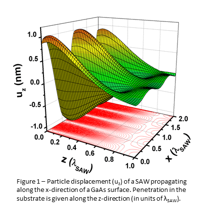
Surface acoustic waves (SAWs) are mechanical vibrations which propagate with a well-defined velocity on the surface of elastic materials. In piezoelectric solids, besides the strain field, a SAW is also characterized by a piezoelectric one. Such an elastic mode decays in amplitude (uz) as it penetrates into the material (z-direction shown in Figure 1), thus concentrating its energy almost totally around the surface.
We employ the energy of SAW modes to modulate and modify the physical properties of semiconductor nanostructures (like quantum wells, quantum dots, and nanowires). The modulation occurs at the SAW frequency which in general ranges from hundreds of MHZ to a few GHz. The SAW fields allow us to modulate single energy levels in low-dimensional structures as well as transport carriers (electrons and holes) and spins in two-dimensional systems. The response of the nanostructures to the acoustic perturbation is investigated using high-resolution optical spectroscopy techniques like CW and time-resolved micro-photoluminescence (m-PL) measurements.
Figure 2(a) illustrates the regions of tension and compression along the SAW propagation direction of a piezoelectric solid. The strain and piezoelectric fields which move with the acoustic velocity (vSAW) modulate the bandgap energy, thus modifying the carrier dynamics of optically created electrons and holes in a semiconductor nanostructure. As depicted in Figure 2(b), the conduction (CB) and valence (VB) band modulation introduced by the SAW creates a type-II energy confinement where energy minima for electrons and holes are spatially separated along the SAW propagation direction. The separation decreases the strength of electron-hole interaction and leads to much longer carrier lifetimes as compared to the case where the SAW is not present.
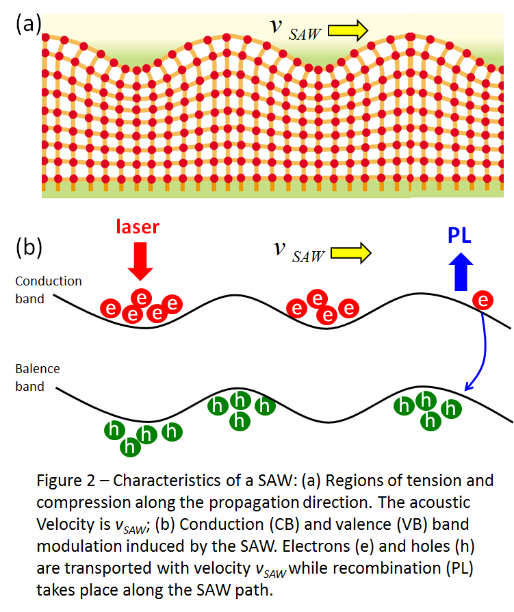
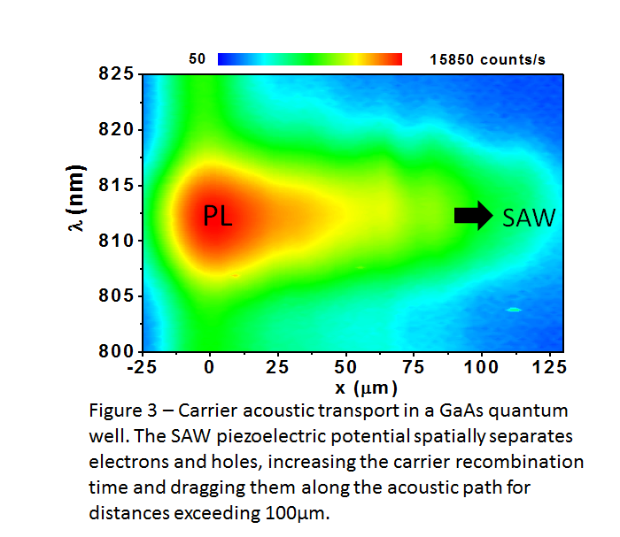
Figure 3 shows a CW PL measurement in a (110) GaAs quantum well under the application of the SAW at 515 MHz. As the SAW propagates along the (001) direction (x direction) along the surface, the piezoelectric potential traps electrons and holes and the longitudinal component of the SAW piezoelectric field drags them along the SAW propagation direction. As we can observe, carriers can be transported at the SAW velocity (vSAW~3000 m/s) over distances exceeding 100 μm, which are much larger than carrier diffusion lengths in such systems.
Using circularly polarized light we are able to prepare the angular momentum state of the incident light on the semiconductor nanostructure. The well-defined angular momentum of the photon is therefore transferred to the electrons in the valence band which, due to the selection rules for angular momentum absorption, are excited in the conduction band with an excess of spin polarization defined by the ratio:![]() where I+ and I– are the PL intensities of the right and left circularly polarized PL emissions.
where I+ and I– are the PL intensities of the right and left circularly polarized PL emissions.
The video below shows a time-resolved PL measurement where I+ and I– are detected simultaneously as a function of time. In this case, carriers are excited with a pulsed laser and the excited carrier packets are seen to propagate along the SAW path (from the top to the bottom direction in the video).
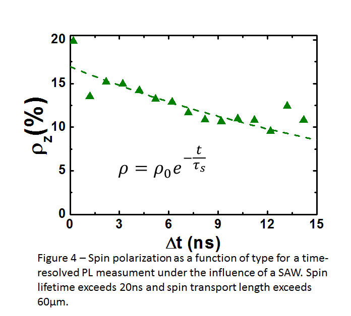
As we observe I+ (which corresponds to emission of electrons with spin up) is more intense than I– (spin down) along the acoustic path. This leads to a net spin polarization been transported by the SAW, which can be summarized in the spin polarization decay curve presented in Figure 4. A fit to an exponential decay leads to a spin relaxation (τs) time of approximately 20 ns, which is about 2 orders of magnitude longer than spin lifetimes obtained in conventional (001) GaAs quantum wells. Besides this, the SAW allows us to define a acoustic transport length defined by Lz=τs*vSAW. In this (110) quantum well Lz > 60μm.


Comentários